Check patentability & draft patents in minutes with Patsnap Eureka AI!

The traceability method of the lamination process section with full traceability of pcb

A process section and whole-process technology, applied in the traceability field of PCB lamination process section, can solve the problem that spraying two-dimensional code cannot monitor and trace the lamination process, achieve good retention and readability, and is not easy Corrosion-resistant, corrosion-resistant and wear-resistant

Active Publication Date: 2022-04-19
深圳镭霆激光科技有限公司
View PDF10 Cites 0 Cited by
  • Summary
  • Abstract
  • Description
  • Claims
  • Application Information

AI Technical Summary

Problems solved by technology

However, in the pressing process, the inner layer information is lost due to the inability to recognize the inner QR code, so that the method of spraying the QR code cannot effectively monitor and trace the pressing process

Method used


Image

  • The traceability method of the lamination process section with full traceability of pcb
  • The traceability method of the lamination process section with full traceability of pcb

Examples


Embodiment Construction

[0016] The following will clearly and completely describe the technical solutions in the embodiments of the present invention with reference to the accompanying drawings in the embodiments of the present invention. Obviously, the described embodiments are only some, not all, embodiments of the present invention. All other embodiments obtained by persons of ordinary skill in the art based on the embodiments of the present invention belong to the protection scope of the present invention.

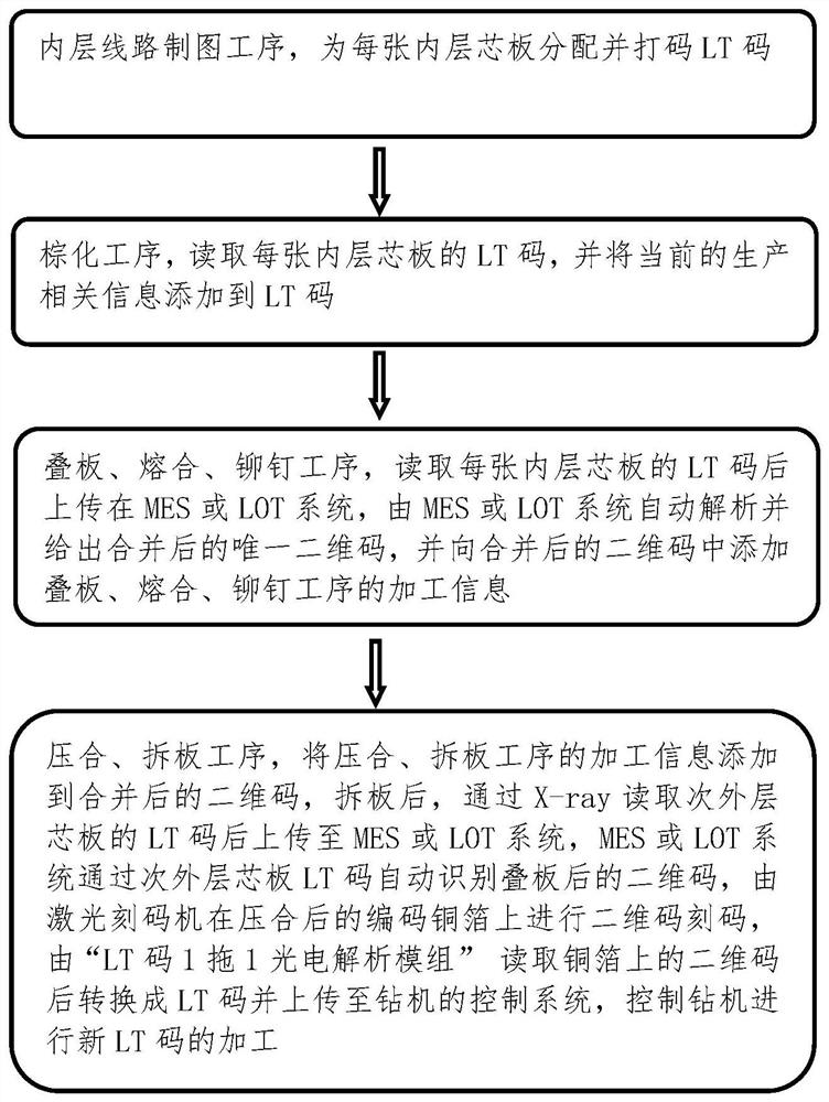
[0017] refer to figure 1 , figure 2 , a method for tracing the laminating process section of the PCB full traceability, comprising the following steps:

[0018] (1) Inner layer circuit design and drawing process, assign a unique LT code to each inner layer core board, and code it on each core board. When etching engineering documents, except for the second outer layer, other inner layer circuits The traceability code area must be etched;

[0019] (2) For the browning process, use the "LT ...


PUM


Abstract

The present invention relates to the technical field of PCB (Printed Circuit Board, printed circuit board), specifically a method for tracing the laminating process section of the PCB, including (1) the inner layer circuit design and drawing process, assigning a unique inner layer core board LT code, and coded on each core board. When etching engineering documents, except for the sub-outer layer, the traceability code area of ​​other inner layer lines must be etched; (2) Pressing process, manual reading when stacking The LT code of each inner core board is uploaded to the MES system or the LOT system, and the MES or LOT system automatically analyzes and gives the combined unique two-dimensional code, and then converts the two-dimensional code into an LT code and prints it on the Press-fit the formed poly into the board. In the lamination process, the present invention combines the LT codes on multiple inner core boards to generate a unique two-dimensional code, and then converts the two-dimensional code into an LT code to be printed on the outer layer to realize the inner layer The transfer of information to the outer layer of information prevents the loss of inner layer information, and can carry out comprehensive and complete monitoring and traceability of the pressing process.

Description

technical field [0001] The invention relates to the technical field of PCB (Printed Circuit Board, printed circuit board), in particular to a traceability method for a pressing process section of a PCB full traceability. Background technique [0002] The basic process flow of PCB is: material cutting—>inner layer circuit—>inner layer AOI (Automatic Optic Inspection, automatic optical inspection)—>pressing—>drilling—>immersion copper plating—>outer layer circuit—>outer layer AOI —>Solder mask—>Text—>Surface treatment—>Forming—>Electrical measurement—>FQC / FQA—>Packaging. In order to quickly identify and correct problems that affect the quality of PCB products, prevent defective products from continuing to flow down the production line, and ultimately achieve zero product return rates, it is necessary to monitor and trace the PCB process. PCB factories generally use two-dimensional code spraying on the board surface, and use scanning g...

Claims


Application Information

Patent Timeline
Patent Type & Authority Patents(China)
IPC IPC(8): G05B19/418G06K17/00
CPCY02P90/02
Inventor 王小兴
Owner 深圳镭霆激光科技有限公司
Features
  • R&D
  • Intellectual Property
  • Life Sciences
  • Materials
  • Tech Scout
  • Unparalleled Data Quality
  • Higher Quality Content
  • 60% Fewer Hallucinations
Learn More