Check patentability & draft patents in minutes with Patsnap Eureka AI!

Gate driving circuit

A gate drive circuit, gate driver technology, applied in electrical components, electronic switches, output power conversion devices, etc., can solve problems such as current unbalance, and achieve the ideal of suppressing current unbalance and suppressing fluctuations in on-off loss. Effect

Active Publication Date: 2019-07-05
MITSUBISHI ELECTRIC CORP
View PDF6 Cites 0 Cited by
  • Summary
  • Abstract
  • Description
  • Claims
  • Application Information

AI Technical Summary

Problems solved by technology

When operating a plurality of semiconductor switching elements connected in parallel, current imbalance occurs due to fluctuations in the characteristics of the elements

Method used


Image

  • Gate driving circuit
  • Gate driving circuit
  • Gate driving circuit

Examples


Embodiment approach 1

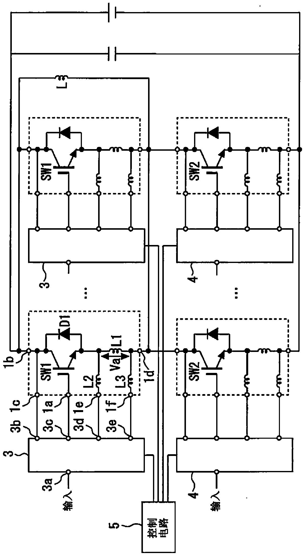
[0017] figure 1 It is a figure which shows the gate drive circuit concerning Embodiment 1 of this invention. The semiconductor switching elements SW1 and SW2 used for power conversion or control are connected in series with each other. A plurality of element pairs of the semiconductor switching elements SW1 and SW2 are connected in parallel. The plurality of gate driver units 3 and 4 respectively drive the plurality of semiconductor switching elements SW1 and SW2 connected in parallel. The inductance L is the load inductance when the semiconductor switching elements SW1 and SW2 are turned on and off. The control circuit 5 controls the plurality of gate driver units 3 , 4 .

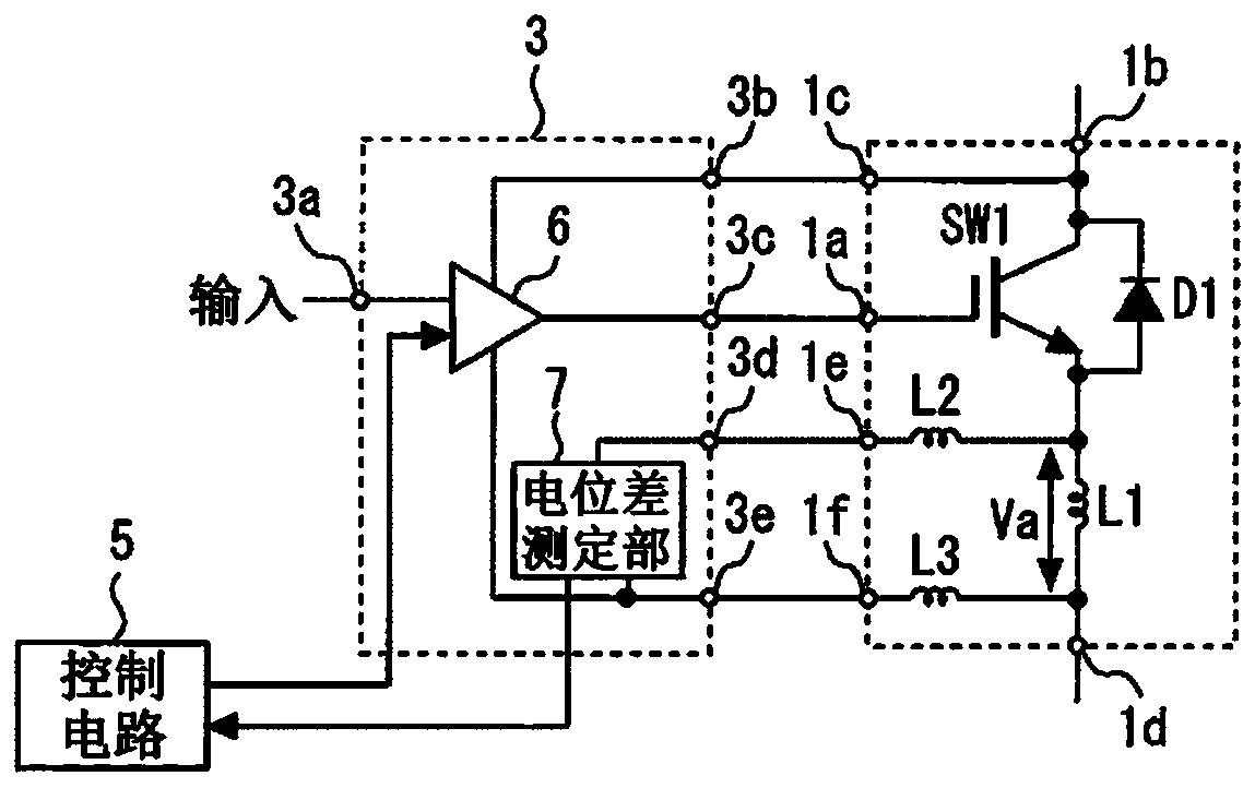
[0018] A diode D1 is connected in antiparallel to the semiconductor switching element SW1. A gate electrode 1a is connected to the gate of the semiconductor switching element SW1. A collector electrode (electrode) 1b and a collector auxiliary electrode 1c are connected to a collector of the semicondu...

Embodiment approach 2

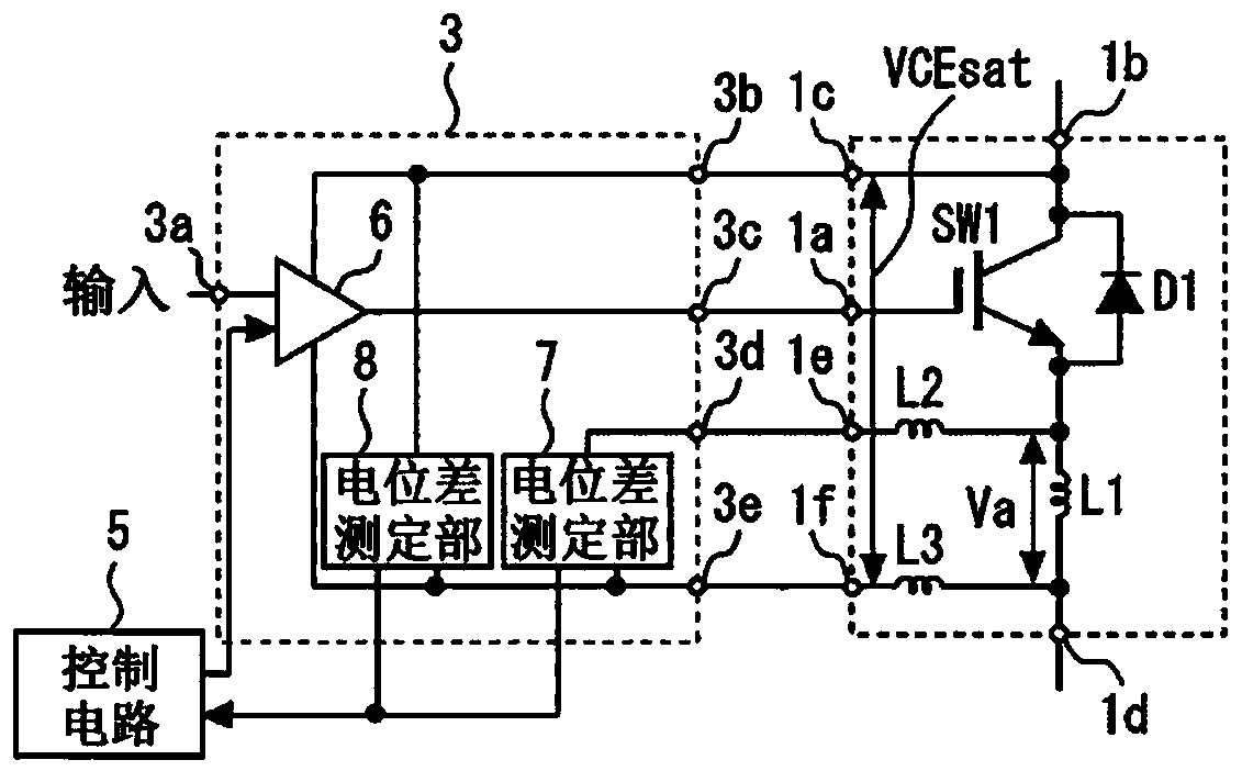
[0027] image 3 It is an enlarged view of a part of the gate drive circuit according to Embodiment 2 of the present invention. The gate driver unit 3 further includes a collector-emitter potential difference measuring unit 8 that connects the collector auxiliary electrode 1c and the emitter auxiliary electrode 1f of the corresponding semiconductor switching element SW1 to each other. The voltage between the collector and the emitter, VCEsat, is measured in units of one cycle of the output frequency. The same applies to the structure of the gate driver unit 4 .

[0028] The control circuit 5 controls the voltages VCEsat supplied from the gate drivers 6 of the respective gate driver units 3 and 4 so that the collector-emitter voltages VCEsat of the plurality of semiconductor switching elements SW1 and SW2 in the steady state are the same as each other. The gate voltage VGE is adjusted. Thereby, it is possible to suppress fluctuations in loss during steady-state ON.

[0029] ...


PUM


Abstract

According to the present invention, a plurality of gate driver units (3, 4) respectively drive a plurality of semiconductor switching elements (SW1, SW2) connected in parallel. A control circuit (5) controls the plurality of gate driver units (3, 4). The gate driver units (3, 4) each have: a gate driver (6) that supplies a gate voltage to gates of the corresponding semiconductor switching elements(SW1, SW2); and a potential difference measuring unit (7) that measures, for each cycle of an output frequency, a potential difference (Va) generated by a wire inductance on an emitter side of the corresponding semiconductor switching elements (SW1, SW2). The control circuit (5) adjusts the gate voltage (VGE), supplied by the gate driver (6) of each of the gate driver units (3, 4), such that potential differences (Va) of the plurality of semiconductor switching elements (SW1, SW2) during a turn-on or turn-off switching operation are equal to each other.

Description

technical field [0001] The present invention relates to a gate drive circuit for driving a plurality of semiconductor switching elements connected in parallel. Background technique [0002] Semiconductor switching elements are used for inverter control of electric railways or electric power transmission. When operating a plurality of semiconductor switching elements connected in parallel, current imbalance occurs due to fluctuations in characteristics between the elements. [0003] Figure 4 It is a diagram showing on-off waveforms of two semiconductor switching elements connected in parallel. Figure 5 It is a diagram showing the off-off waveforms of two semiconductor switching elements connected in parallel. I1 and I2 are the currents flowing through the two semiconductor switching elements, VGE is the gate-emitter voltage, and VCE is the collector-emitter voltage. from Figure 4 , 5 It can be seen that the currents I1 and I2 are unbalanced. [0004] Patent Document 1...

Claims


Application Information

Patent Timeline
Patent Type & Authority Applications(China)
IPC IPC(8): H03K17/567H02M1/08
CPCH02M1/088H03K17/165H03K2217/0036H02M1/0009H03K17/567H03K17/6871H02M1/08
Inventor 齐藤升太中本启介
Owner MITSUBISHI ELECTRIC CORP
Features
  • R&D
  • Intellectual Property
  • Life Sciences
  • Materials
  • Tech Scout
  • Unparalleled Data Quality
  • Higher Quality Content
  • 60% Fewer Hallucinations
Learn More