Unlock instant, AI-driven research and patent intelligence for your innovation.

On-chip debugging device and method

An on-chip debugging and debugger technology, applied in measurement devices, using configuration tests to detect faulty hardware, instruments, etc., can solve problems such as lack of auxiliary debugging, large amount of data, and difficulty in implementation, so as to facilitate discovery, resolution, and occupation. Low-resource, powerful effects

Inactive Publication Date: 2019-07-19
SUZHOU CENTEC COMM CO LTD
View PDF14 Cites 15 Cited by
  • Summary
  • Abstract
  • Description
  • Claims
  • Application Information

AI Technical Summary

Problems solved by technology

For on-chip debugging of dedicated chips, the above techniques are more difficult to implement, and there is currently no external debugger available to parse the input / output information of the JTAG interface
[0008] (2) Existing debugging method 2
Although the technical solution in Patent Document 3 includes a trigger control function, it can only start tracking data after the trigger condition is met. Generally, when an error occurs during operation of a chip and needs to be debugged, the trigger conditions that can be set are all It is the moment after the error occurs, so the traced data in this case can only be the data after the error occurs, and the data really needed for debugging should be the data before the error occurs
Especially when an error occurs during the long-term operation of the chip, it is difficult to analyze the cause of the error if the debugging method of Patent Document 3 is used
The technical solution in Patent Document 3 also provides the function of outputting tracking data externally, but because the tracked data in this technical solution is unconditionally tracked after the trigger condition is met, there is no special distinction between the information that is effective for debugging and the sampled data The amount is large, and the performance requirements of the output interface are high, which is not conducive to the specific hardware design of this technology
[0012] (3) Existing debugging method three
When an error occurs in the normal operation of the chip, online design is needed. This solution is powerless and does not play any role in auxiliary debugging.

Method used


Image

  • On-chip debugging device and method
  • On-chip debugging device and method
  • On-chip debugging device and method

Examples


Embodiment 1

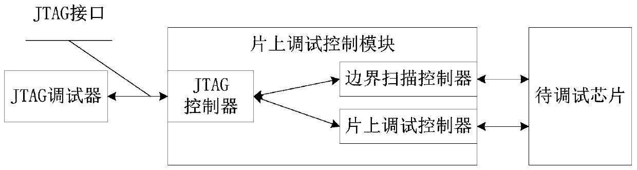
[0035] Overall structure of technical scheme of the present invention is as Figure 4 shown. An on-chip debugging control module is added to the chip to be debugged. This module mainly includes several parts: external interface module, debugging mode control module, debugging information processing module, debugging monitoring module, time generator, and two debugging memories, a relatively small fast memory and a relatively large slow memory. fast memory. The external interface module is used for outputting chip debugging status information to an external debugger and receiving control commands from the external debugger. Wherein, the debugging mode control module is used to set the to-be-sampled type of the internal signal of the specified chip according to the debugging configuration of the external debugger or the internal CPU, and to set the debugging trigger condition; the debugging monitoring module is used to sample and record the chip of the specified type The inte...

Embodiment 2

[0048] The embodiment of the invention also discloses an on-chip debugging method. Such as Figure 5 As shown, the on-chip debugging method includes the following steps:

[0049] Step S101, according to the configuration of the external debugger or the chip to be debugged, determine the sampling type and the triggering condition for debugging.

[0050] The external debugger or the on-chip CPU of the chip to be debugged configure the working mode of the on-chip debugging function module: specify the internal signal of the chip to be sampled, set the size of the fast and slow memory inside the on-chip debugging module, set the conditions for starting the on-chip debugging function, and set the on-chip The condition for the end of the debugging function, set the format of the debugging status information stored in the internal memory, set the format when the debugging status information needs to be output, and set the subsequent working mode of the debugging module and the chip ...


PUM


Abstract

The invention discloses an on-chip debugging device and method, and the device comprises an external interface module which is used for outputting the debugging state information of a chip to an external debugger, and receiving a control instruction of the external debugger; a debugging mode control module which is used for setting a to-be-sampled type of an internal signal of a specified chip according to the debugging configuration of the external debugger or the internal CPU, and setting a debugging trigger condition; a debugging monitoring module which is used for sampling and recording the internal signals of the chip of the specified type so as to identify the operation state of the chip; and a debugging information processing module which is used for storing the running state of thechip into an internal debugging memory, and sending the running state of the chip to the external debugger through the external interface module or sending the running state of the chip to an internal CPU through an internal bus. By means of the device and the method, the chip on-chip debugging function which is relatively simpler, occupies fewer resources and has more powerful functions can be achieved.

Description

technical field [0001] The invention relates to chip debugging technology, in particular to an on-chip debugging device and method. Background technique [0002] With the continuous improvement of technology, the design of integrated circuit chips is becoming more and more complicated. The area of ​​each chip is constantly increasing, and more and more logics are integrated in it, and the functions are becoming more and more complex, thus putting forward higher requirements for chip verification. The pre-verification of the chip in the design process, including simulation verification and prototype verification, has been difficult to fully guarantee the correctness of the chip. In addition, the chip has various configurations and working modes during use, and a little carelessness may cause problems. unpredictable consequences. Therefore, debugging on real chips becomes more and more important. The efficiency of on-chip debugging also greatly affects the stability of the ...

Claims


Application Information

Patent Timeline
Patent Type & Authority Applications(China)
IPC IPC(8): G06F11/22
CPCG06F11/221G06F11/2289G01R31/31705G01R31/318597G01R31/3187G06F11/3089
Inventor 贾复山姜瑞张继存
Owner SUZHOU CENTEC COMM CO LTD