Method for producing semiconductor chips
一种制造方法、半导体的技术,应用在半导体/固态器件制造、半导体器件、制造工具等方向,能够解决芯片角缺损等问题,达到可靠除去、抑制不合格芯片的产生、抑制芯片成本的效果
- Summary
- Abstract
- Description
- Claims
- Application Information
AI Technical Summary
Problems solved by technology
Method used
Image

Examples
no. 1 Embodiment approach
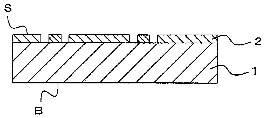
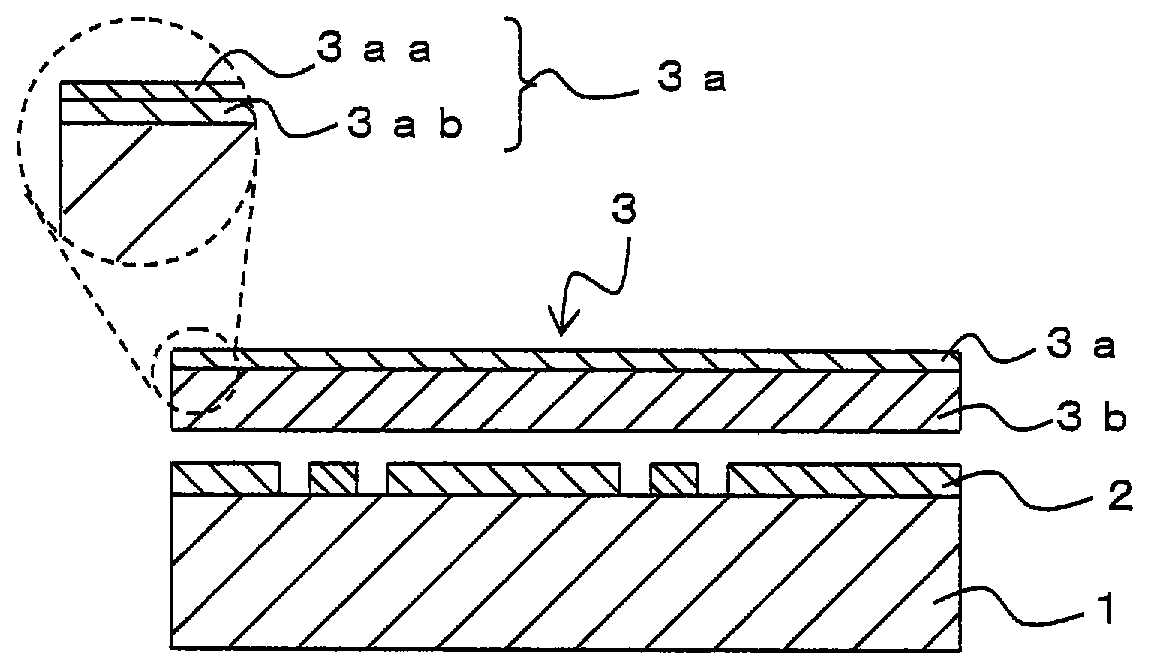
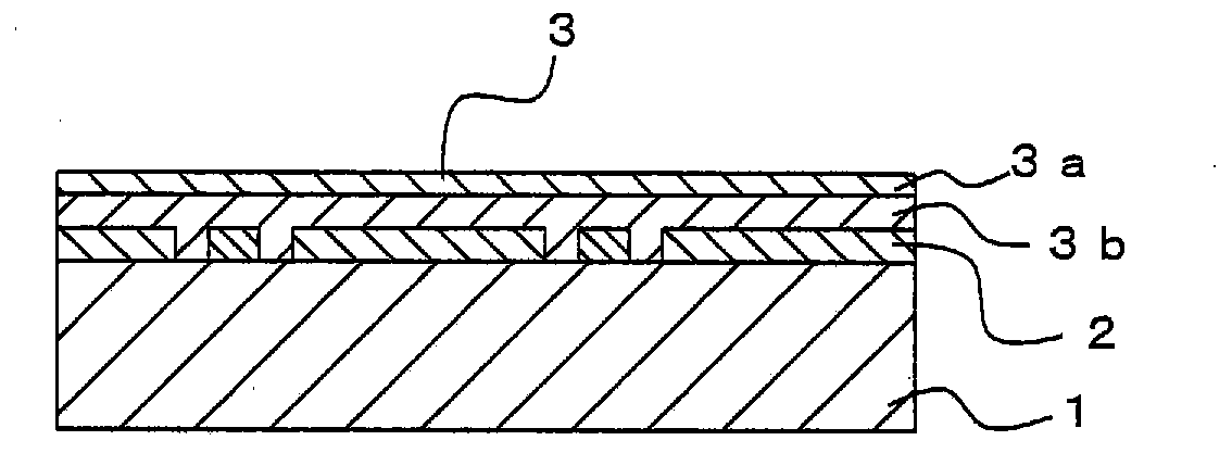
[0057] A first embodiment of the production method of the present invention will be described with reference to FIGS. 1 to 5 . Semiconductor wafer 1 has on its surface S pattern surface 2 (refer to Figure 1A ). On the pattern surface 2 side of the semiconductor wafer 1, the mask-integrated surface protection tape 3 (refer to Figure 1B ). Thus, the semiconductor wafer 1 whose pattern surface 2 is covered with the mask-integrated surface protection tape 3 (refer to Figure 1C ).
[0058] The mask-integrated surface protection tape 3 is configured by further providing a mask material layer 3b on the adhesive layer 3ab of the surface protection tape 3a provided with the adhesive layer 3ab on the base film 3aa. That is, the mask-integrated surface protection tape 3 has a surface protection tape 3 a and a mask material layer 3 b provided on the surface protection tape 3 a. In addition, in the mask-integrated surface protection tape 3, each of the base film 3aa, the adhesive la...
no. 2 Embodiment approach
[0109] exist Figure 6A ~ Figure 6C The second embodiment shown differs from the first embodiment in that it includes irradiating the mask-integrated surface protection tape 3 with ultraviolet light before the step of peeling off the surface protection tape 3 a in the first embodiment. A step of curing the adhesive layer 3ab by radiation. Other steps are the same as those of the first embodiment.
[0110] That is, first, the mask-integrated surface protection tape 3 is pasted on the surface S side of the semiconductor wafer 1, and the wafer fixing tape 4 is pasted on the ground back side B side of the semiconductor wafer 1, and supported and fixed on the ring frame 13 ( refer to Figure 2C , Figure 6A ). Then, the mask-integrated surface protection tape 3 is irradiated with ultraviolet rays (UV19) from the surface S side (see Figure 6B ). Then, after the adhesive layer 3ab of the mask-integrated surface protection tape 3 is cured, the surface protection tape 3a is remo...
Embodiment 1
[0124] Using the mask-integrated surface protection tape 3 obtained above, a semiconductor wafer 1 is processed. As the remover 16 of the mask material layer 3b, methyl ethyl ketone (MEK) was sprayed.
PUM
| Property | Measurement | Unit |
|---|---|---|
| visible light transmittance | aaaaa | aaaaa |
| visible light transmittance | aaaaa | aaaaa |
| visible light transmittance | aaaaa | aaaaa |
Abstract
Description
Claims
Application Information
 - R&D
- Intellectual Property
- Life Sciences
- Materials
- Tech Scout
- Unparalleled Data Quality
- Higher Quality Content
- 60% Fewer Hallucinations
Browse by: Latest US Patents, China's latest patents, Technical Efficacy Thesaurus, Application Domain, Technology Topic, Popular Technical Reports.
© 2025 PatSnap. All rights reserved.Legal|Privacy policy|Modern Slavery Act Transparency Statement|Sitemap|About US| Contact US: help@patsnap.com