Supercharge Your Innovation With Domain-Expert AI Agents!

A kind of LED display panel, its preparation method and display device

A display panel and LED chip technology, applied in semiconductor devices, electrical components, circuits, etc., can solve problems such as uneven exposure, and achieve the effect of improving the uniformity of light output and ensuring consistent light output efficiency.

Active Publication Date: 2021-01-22
BOE TECH GRP CO LTD
View PDF6 Cites 0 Cited by
  • Summary
  • Abstract
  • Description
  • Claims
  • Application Information

AI Technical Summary

Problems solved by technology

[0007] In view of this, an embodiment of the present invention provides an LED display panel, its manufacturing method and a display device to solve the problem of uneven exposure in the prior art

Method used


Image

  • A kind of LED display panel, its preparation method and display device
  • A kind of LED display panel, its preparation method and display device
  • A kind of LED display panel, its preparation method and display device

Examples


preparation example Construction

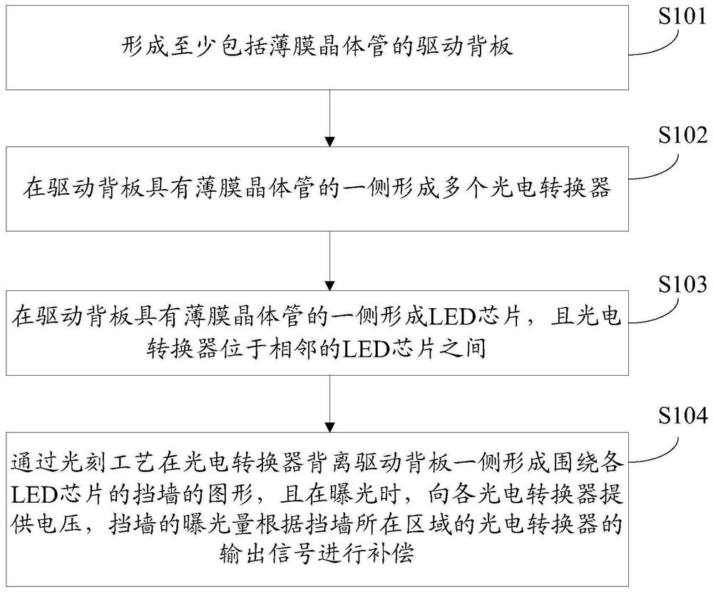
[0038] A kind of preparation method of LED display panel provided by the embodiment of the present invention, such as figure 1 shown, including:

[0039] S101, forming a driving backplane including at least thin film transistors;

[0040] S102, forming a plurality of photoelectric converters on the side of the driving backplane with thin film transistors;

[0041] S103, forming LED chips on the side of the driving backplane with thin film transistors, and the photoelectric converters are located between adjacent LED chips;

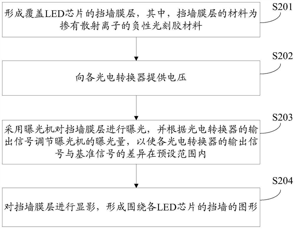
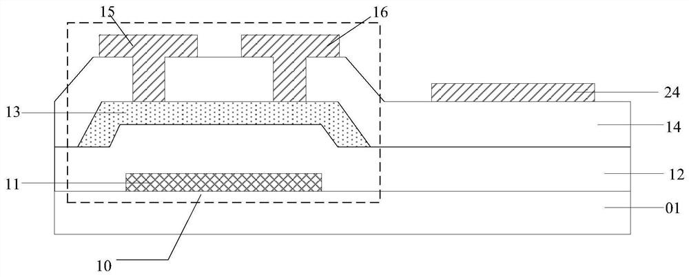
[0042] S104. Form the pattern of the barrier wall surrounding each LED chip on the side of the photoelectric converter away from the driving backplane through the photolithography process, and provide voltage to each photoelectric converter during exposure, and the exposure amount of the barrier wall depends on the area where the barrier wall is located. The output signal of the photoelectric converter is compensated; the closer to the surface of the dri...


PUM

PropertyMeasurementUnit
sizeaaaaaaaaaa

Abstract

A display panel, a preparation method therefor, and a display device, the display panel comprising: a driving backplane, the driving backplane comprising a base substrate (01) and a plurality of photoelectric converters (20) located on the base substrate (01); a plurality of light-emitting diode chips (30) located on the driving backplane; and a retaining wall (51) located on the driving backplane. The retaining wall (51) is located between adjacent light-emitting diode chips (30); the photoelectric converter (20) is located between adjacent light-emitting diode chips (30); and the photoelectric converter (20) is configured to detect the amount of exposure in a process of photolithography processing for manufacturing the retaining wall (51).

Description

technical field [0001] The invention relates to the field of display technology, in particular to an LED display panel, a preparation method thereof and a display device. Background technique [0002] With the development of technology and the requirements for display, Micro-LED (Micro Light Emitting Diode, Micro-LED) is the development trend of display devices in the future. High contrast, ultra-high color gamut, high luminous efficiency, high brightness, low energy consumption, etc. [0003] Take a standard 3840ⅹ2160 resolution display screen as an example, with a total of 8,294,400 pixels. For RGB Micro-LEDs, a total of 2,488,3200 Micro-LED chips are required, and the chip size is only about 1 μm to 10 μm. At present, the chips are first on the sapphire substrate. After it is done, it will be transferred to the driver backplane by mass transfer method, but the mass transfer technology is still immature, and the yield rate is low. According to the standard of 99.99% yield...

Claims


Application Information

Patent Timeline
Patent Type & Authority Patents(China)
IPC IPC(8): H01L27/15
CPCH01L27/156
Inventor 于勇舒适岳阳黄海涛李翔徐传祥
Owner BOE TECH GRP CO LTD
Features
  • R&D
  • Intellectual Property
  • Life Sciences
  • Materials
  • Tech Scout
  • Unparalleled Data Quality
  • Higher Quality Content
  • 60% Fewer Hallucinations
Learn More