Supercharge Your Innovation With Domain-Expert AI Agents!

Trench silicon carbide mosfet device with low power consumption and high reliability

A reliable, trench-type technology, applied to semiconductor devices, electrical components, circuits, etc., can solve problems such as weak short-circuit capability, high switching loss, and large gate-to-drain capacitance, so as to reduce saturation current, reduce switching loss, and improve The effect of short circuit capability

Active Publication Date: 2021-07-02
UNIV OF ELECTRONICS SCI & TECH OF CHINA
View PDF0 Cites 0 Cited by
  • Summary
  • Abstract
  • Description
  • Claims
  • Application Information

AI Technical Summary

Problems solved by technology

Although the P+ shielding layer at the bottom of the trench gate can strongly protect the oxide layer at the bottom and corners of the trench gate, the oxide layer on the sidewall of the trench will still be challenged by a high electric field in the blocking state, so the P+ shielding layer The introduction cannot completely solve the reliability problem that the trench gate oxide layer is impacted by high electric field
[0005] Due to the poor interface state between the current silicon carbide material and the gate oxide dielectric, the channel mobility is too low, and the conduction characteristics of the trench gate silicon carbide MOSFET are still far from the theoretical limit.
Due to the large gate-to-drain capacitance of the trench-gate SiC MOSFET, its switching loss is high
At the same time, due to its high current saturation current, its short-circuit capability is weak

Method used


Image

  • Trench silicon carbide mosfet device with low power consumption and high reliability
  • Trench silicon carbide mosfet device with low power consumption and high reliability
  • Trench silicon carbide mosfet device with low power consumption and high reliability

Examples


Embodiment 1

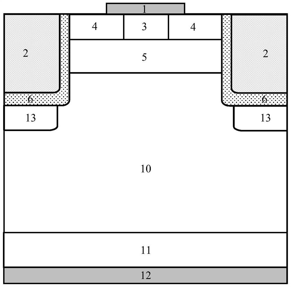
[0026] Such as figure 2 As shown, a trench type silicon carbide MOSFET device with low power consumption and high reliability in this embodiment includes: an N-type substrate 11, an N-type epitaxial layer 10 located above the N-type substrate 11, and an N-type epitaxial layer 10 located on the N-type epitaxial layer. The second P-body region 9 above the layer 10, the second P+ contact region 7 and the second N+ contact region 8 located inside the second P-body region 9, the second P+ contact region 7 and the second N+ contact region 8 The upper source electrode 1, the gate dielectric 6 above the second N+ contact region 8 and the groove gate 2 inside the gate dielectric 6, the first P-body region 5 between the gate dielectric 6, and the first P-body region 5 above the two first N+ contact regions 4, the first P+ contact region 3 between the two first N+ contact regions 4, the source electrode 1 above the first P+ contact region 3 and the first N+ contact region 4, The drain ...

Embodiment 2

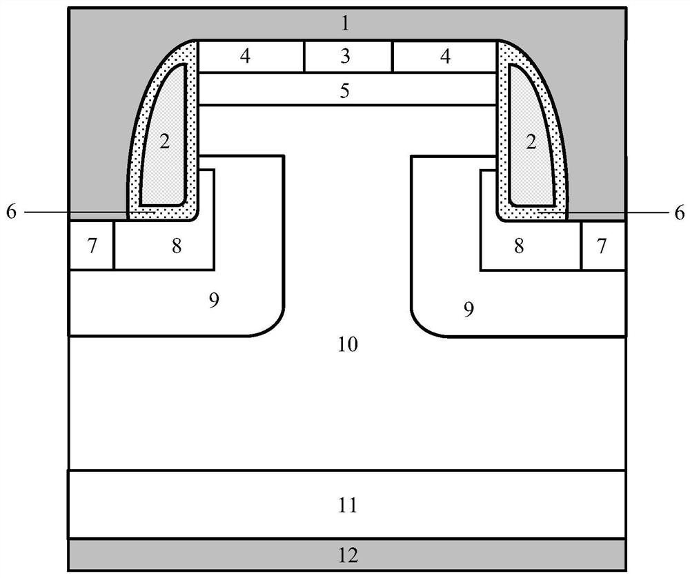
[0030] Such as image 3As shown, the difference between the device structure of this embodiment and Embodiment 1 is that the trench gate 2 and the gate dielectric 6 are in an inverted L shape, and the inverted L shape includes a horizontal section and a vertical section connected below the horizontal section. An N-type epitaxial layer 10 is provided between a P-body region 5 and gate dielectrics 6 on both sides, and the horizontal section of the trench gate 2 and gate dielectric 6 is located in the first N+ contact region 4, the first P-body region 5 and the N Above the N-type epitaxial layer 10 , a gate dielectric 6 is provided between the trench gate 2 and the first N+ contact region 4 , the first P-body region 5 , and the N-type epitaxial layer 10 .

Embodiment 3

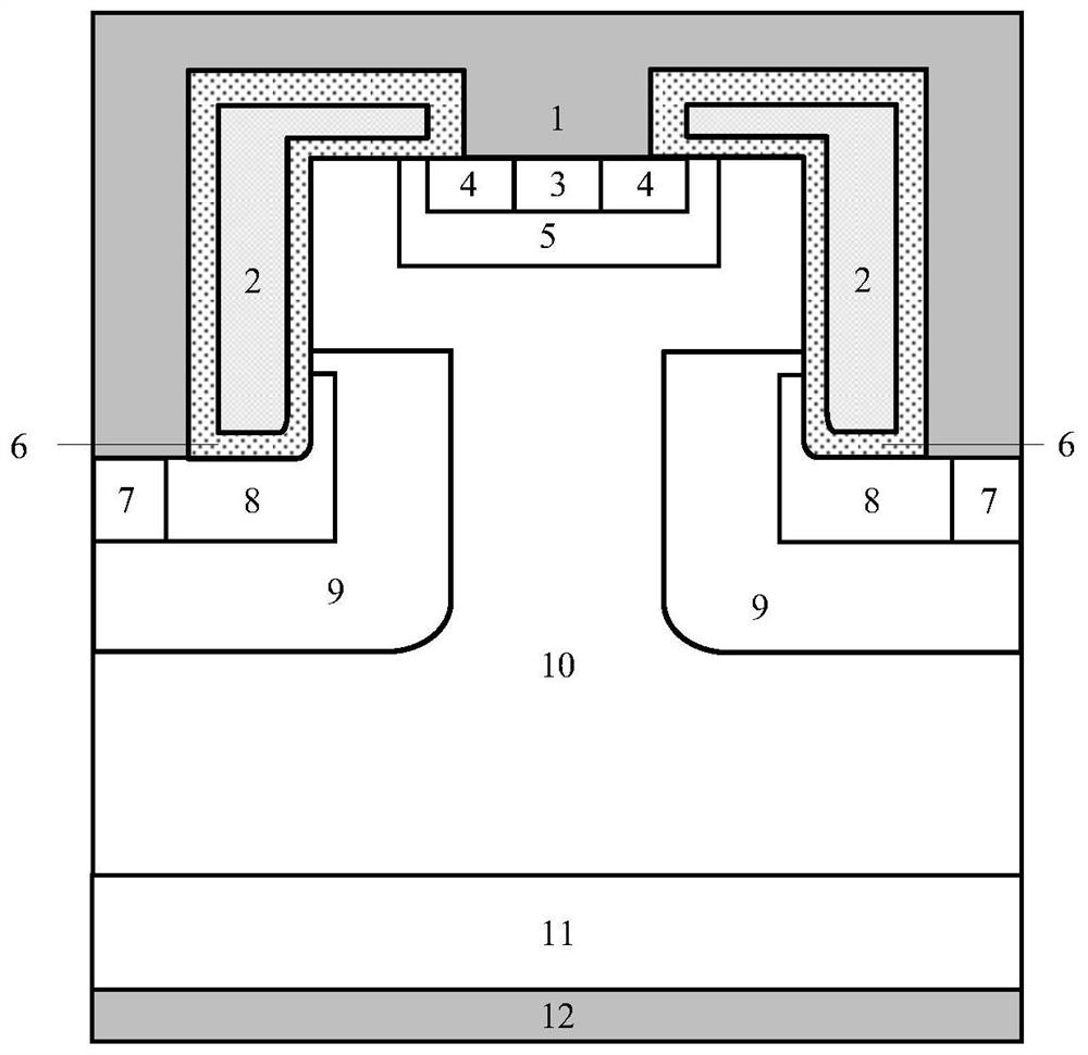
[0032] Such as Figure 4 As shown, two first P-body regions 5 are arranged between gate dielectrics 6, two first P+ contact regions 3 are arranged between two first N+ contact regions 4, and two first P+ contact regions 3 are arranged An N-type epitaxial layer 10 is provided between the first P-body regions 5 and between the two first P-body regions 5 , and the N-type epitaxial layer 10 forms a Schottky contact with the source electrode 1 . The advantage of doing this is that the performance of the third quadrant of the device is improved.


PUM


Abstract

The present invention provides a trench silicon carbide MOSFET device with low power consumption and high reliability, comprising: an N-type substrate, an N-type epitaxial layer, a first P-body region, a first P+ contact region, and a first N+ contact region , the second P-body region, the second P+ contact region, the second N+ contact region, oxide layer, groove gate, metal electrode, drain; the SiC MOSFET device proposed by the present invention significantly reduces the on-resistance through parallel connection of 4 channels , through the second P-body wrapping and protecting the gate groove, it not only enhances the reliability of the oxide layer of the device, but also shields part of the gate-drain capacitance to reduce the switching loss of the device; when the device is short-circuited, the first P-body The pinch-off of the JFET region formed by the region and the second P-body region reduces the saturation current of the device and improves its short-circuit capability.

Description

technical field [0001] The invention belongs to the technical field of power semiconductor devices, in particular to a trench type silicon carbide MOSFET device with low power consumption and high reliability. Background technique [0002] As one of the representatives of the third-generation wide bandgap semiconductor materials, silicon carbide (Silicon Carbide) material has a large bandgap (3.26eV) and a high critical electric field (3×10 6 V / cm), high carrier saturation drift velocity (2×10 7 cm / s), high thermal conductivity (490W / Mk), and good thermal stability. It is an excellent material for the preparation of high-voltage power electronic devices. Application prospect. [0003] MOSFET is the most widely used gate-controlled device structure in silicon carbide power devices. Since silicon carbide MOSFET is a device characterized by unipolar transport working mechanism, only one kind of carrier in electrons or holes conducts electricity, and there is no charge storag...

Claims


Application Information

Patent Timeline
Patent Type & Authority Patents(China)
IPC IPC(8): H01L29/10H01L29/06H01L29/16H01L29/78
CPCH01L29/0684H01L29/1037H01L29/1608H01L29/7827
Inventor 李轩徐晓杰黄伟陈致宇邓小川张波
Owner UNIV OF ELECTRONICS SCI & TECH OF CHINA
Features
  • R&D
  • Intellectual Property
  • Life Sciences
  • Materials
  • Tech Scout
  • Unparalleled Data Quality
  • Higher Quality Content
  • 60% Fewer Hallucinations
Learn More