Packaging method and packaging structure of integrated antenna
A technology of integrated antenna and packaging method, which is applied in the direction of antenna support/mounting device, antenna grounding switch structure connection, antenna, etc., can solve the problems of integrated antenna preparation precision limitation, achieve the goal of reducing size and improving placement accuracy Effect
- Summary
- Abstract
- Description
- Claims
- Application Information
AI Technical Summary
Problems solved by technology
Method used
Image

Examples
Example Embodiment
[0034] Example 1
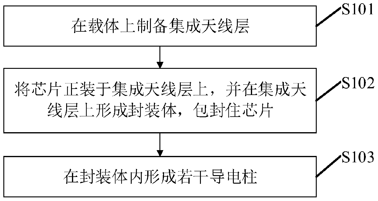
[0035] This embodiment provides a packaging method for an integrated antenna, such as figure 1 shown, including the following steps:
[0036] Step S101: preparing an integrated antenna layer on a carrier.
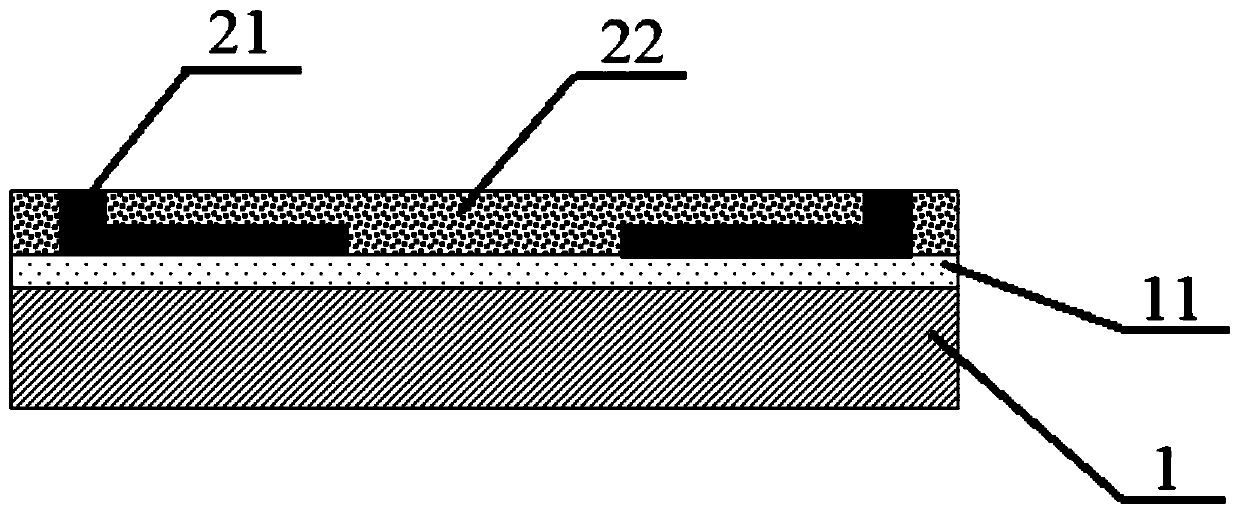
[0037] here, as figure 2 As shown, the integrated antenna layer 2 includes an antenna 21 and a dielectric layer 22 covering the antenna 21 , and the interface of the antenna 21 is exposed outside the dielectric layer 22 .
[0038] Here, in order to remove the carrier 1 after performing all the steps of the method in the embodiment of the present invention and completing the preparation of the package structure of the integrated chip 3, as figure 2 As shown, a sacrificial layer 11 can be provided on the carrier 1 first, and then the integrated antenna layer 2 can be prepared on the sacrificial layer 11. Specifically, the sacrificial layer 11 can be an adhesive layer, for example, a high temperature bonding adhesive layer or a UV adhesive film Wait. ...
Example Embodiment
[0088] Example 2
[0089] This embodiment provides a wafer-level fan-out packaging structure, which is prepared according to the above-mentioned embodiment 1 and its preferred implementation manners, and what has been explained will not be repeated here.
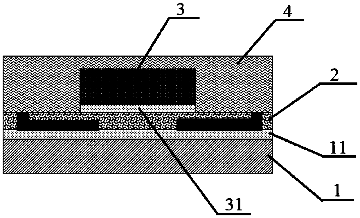
[0090] The packaging structure of the integrated antenna provided in this embodiment, such as Figure 7 As shown, it includes: an integrated antenna layer 2, a chip 3, a package body 4 and conductive pillars.
[0091] Among them, the integrated antenna layer 2 includes an antenna 21 and a dielectric layer 22 covering the antenna 21, and the antenna interface of the antenna 21 is exposed outside the dielectric layer 22; the package body 4 is arranged on the integrated antenna layer 2, and the chip 3 is packaged in the package body 4 , the device surface of the chip 3 is away from the integrated antenna layer 2; the package body 4 also includes a number of conductive columns, the conductive columns include the first conductiv...
PUM
 Abstract
Description
Claims
Application Information
 - R&D Engineer
- R&D Manager
- IP Professional
- Industry Leading Data Capabilities
- Powerful AI technology
- Patent DNA Extraction
Browse by: Latest US Patents, China's latest patents, Technical Efficacy Thesaurus, Application Domain, Technology Topic.
© 2024 PatSnap. All rights reserved.Legal|Privacy policy|Modern Slavery Act Transparency Statement|Sitemap