High-efficiency photovoltaic solder strip
A photovoltaic ribbon, a high-efficiency technology, applied in photovoltaic power generation, electrical components, circuits, etc., can solve the problem of reduced reflective reuse ability, achieve the effect of optimizing the reflective reuse rate and increasing the effective reflective reuse area
- Summary
- Abstract
- Description
- Claims
- Application Information
AI Technical Summary
Problems solved by technology
Method used
Image

Examples
Embodiment 1
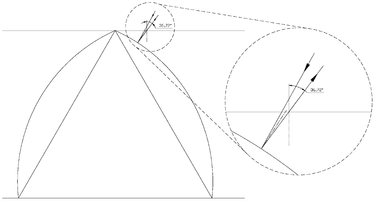
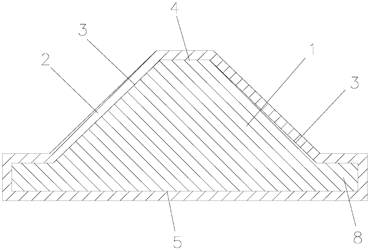
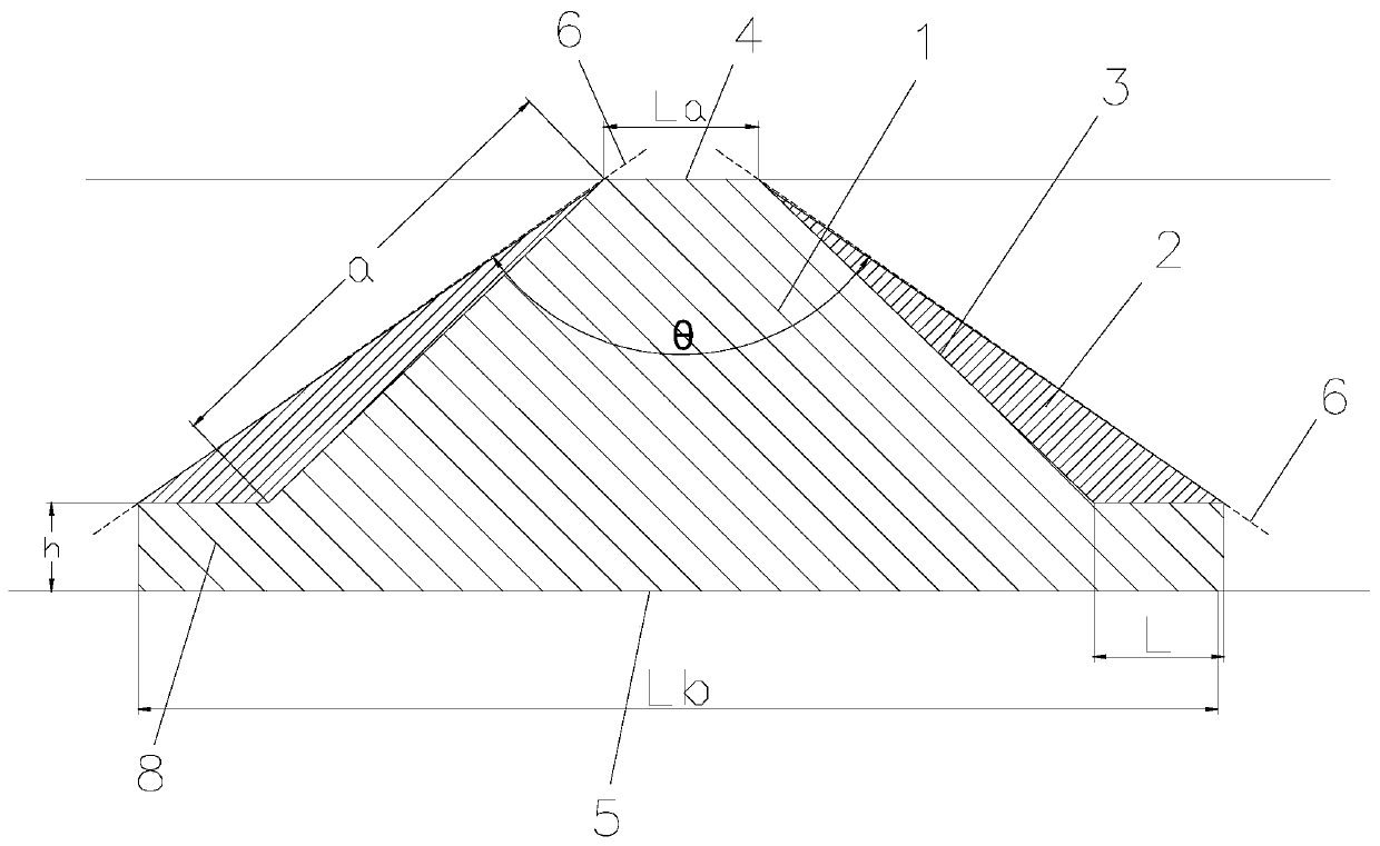
[0054] like figure 2 , image 3 and Figure 4 As shown, a high-efficiency photovoltaic welding ribbon: includes a conductive base strip 1, the conductive base strip 1 is covered with a solder layer 2, the conductive base strip 1 has two sides 3, and the upper ends of the two sides 3 are close to each other to form a narrow portion 4. The lower ends are far away from each other to form a wide part 5. At least one reunion structure is provided on both sides of the conductive base tape 1, so that the outer surface covered on the side surface 3 of the conductive base tape 1 approaches an inclined plane. The inclined plane is the predetermined An effective reflective surface 6 is provided;
[0055] The agglomeration structure includes a fin part 8 arranged at the bottom of the side 3, the upper surface of the fin part 8 is docked with the side 3 on the side where it is located, the side 3 is a slope inclined outward from top to bottom, and the upper surface of the fin part 8 is ...
Embodiment 2
[0062] like Figure 7 and Figure 8 As shown, a high-efficiency photovoltaic welding ribbon: includes a conductive base strip 1, the conductive base strip 1 is covered with a solder layer 2, the conductive base strip 1 has two sides 3, and the upper ends of the two sides 3 are close to each other to form a narrow portion 4. The lower ends are far away from each other to form a wide part 5. At least one reunion structure is provided on both sides of the conductive base tape 1, so that the outer surface covered on the side surface 3 of the conductive base tape 1 approaches an inclined plane. The inclined plane is the predetermined An effective reflective surface 6 is provided;
[0063] The agglomeration structure is an inwardly recessed agglomeration groove 7 on the side surface 3 .
[0064] There are at least two agglomeration grooves 7 on each side 3 at intervals, and the cross-sectional shape of the agglomeration groove 7 is arc-shaped, V-shaped or trapezoidal, wherein the ...
Embodiment 3
[0069] like Figure 9 and Figure 10 As shown, a high-efficiency photovoltaic welding ribbon: includes a conductive base strip 1, the conductive base strip 1 is covered with a solder layer 2, the conductive base strip 1 has two sides 3, and the upper ends of the two sides 3 are close to each other to form a narrow portion 4. The lower ends are far away from each other to form a wide part 5. At least one reunion structure is provided on both sides of the conductive base strip 1, so that the outer surface covered on the side 3 of the conductive base strip 1 approaches an inclined plane after the automatic serial welding is completed. The inclined plane is the preset effective reflective surface 6;
[0070] The agglomeration structure is an inwardly recessed agglomeration groove 7 on the side surface 3 .
[0071] There is one agglomeration groove 7 on each side 3, and the cross-sectional shape of the agglomeration groove 7 is arc-shaped, V-shaped or trapezoidal, and connects th...
PUM
| Property | Measurement | Unit |
|---|---|---|
| height | aaaaa | aaaaa |
| width | aaaaa | aaaaa |
| length | aaaaa | aaaaa |
Abstract
Description
Claims
Application Information
 - R&D
- Intellectual Property
- Life Sciences
- Materials
- Tech Scout
- Unparalleled Data Quality
- Higher Quality Content
- 60% Fewer Hallucinations
Browse by: Latest US Patents, China's latest patents, Technical Efficacy Thesaurus, Application Domain, Technology Topic, Popular Technical Reports.
© 2025 PatSnap. All rights reserved.Legal|Privacy policy|Modern Slavery Act Transparency Statement|Sitemap|About US| Contact US: help@patsnap.com