3D Laminated Semiconductor Device
A semiconductor and stacking technology, applied in the direction of semiconductor devices, semiconductor/solid-state device parts, electrical components, etc., can solve the problems of increasing the difficulty of landing, increasing the resistance value, reducing the resistance value, etc.
- Summary
- Abstract
- Description
- Claims
- Application Information
AI Technical Summary
Problems solved by technology
Method used
Image

Examples
Embodiment Construction
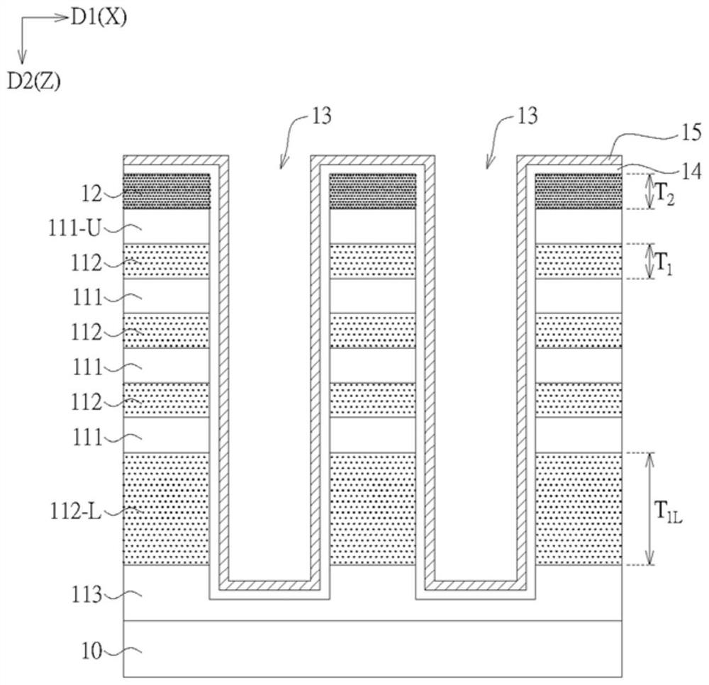
[0051] In an embodiment of the disclosure, a three-dimensional stacked semiconductor device is provided. According to the structure arrangement proposed in the embodiment, the pad structure of the contact via landing can be improved and the resistance value of the contact via can be reduced, and there is no need to perform additional plugs (such as bit line N+ plugs) on the stacked structure as in the conventional structure. ) process and N+ ion implantation. Furthermore, according to the manufacturing method proposed in the embodiment, the fabrication of the improved pad structure is performed simultaneously with the patterning step of the OP stack layer, and no additional yellow light process is required. Therefore, the three-dimensional stacked semiconductor device of the embodiment can not only improve its electronic properties (e.g. reduce the resistance value), but also can be fabricated with simple, less process and less expensive processes.
[0052] The embodiments of...
PUM
| Property | Measurement | Unit |
|---|---|---|
| thickness | aaaaa | aaaaa |
Abstract
Description
Claims
Application Information
 - R&D
- Intellectual Property
- Life Sciences
- Materials
- Tech Scout
- Unparalleled Data Quality
- Higher Quality Content
- 60% Fewer Hallucinations
Browse by: Latest US Patents, China's latest patents, Technical Efficacy Thesaurus, Application Domain, Technology Topic, Popular Technical Reports.
© 2025 PatSnap. All rights reserved.Legal|Privacy policy|Modern Slavery Act Transparency Statement|Sitemap|About US| Contact US: help@patsnap.com