A method for improving ILD oxide layer spalling
An oxide layer, crystal edge technology, applied in electrical components, semiconductor/solid-state device manufacturing, circuits, etc., can solve problems such as blocking holes, collapse, aluminum metal residues, etc.
- Summary
- Abstract
- Description
- Claims
- Application Information
AI Technical Summary
Problems solved by technology
Method used
Image

Examples
Embodiment Construction
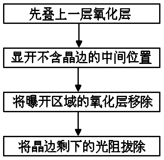
[0012] to combine figure 1 As shown, the method for improving the peeling off of the ILD oxide layer is implemented in the following embodiments by adopting the following technical scheme:
[0013] Step 1, after ILDOCMP, stack an oxide layer earlier, and the thickness of the oxide layer stacked is
[0014] Step 2. Apply photoresist and expose to reveal the middle position without crystal edge. The radius of the crystal edge revealed is greater than 147mm.
[0015] Step 3, removing the oxide layer in the exposed area. Etching is used to remove the oxide layer, and the height of the gate should not be damaged during specific implementation.
[0016] Step 4. Remove the remaining photoresist on the edge of the crystal to thicken the oxide layer on the remaining edge of the crystal.
[0017] The present invention has been described in detail through specific embodiments above, but these do not constitute a limitation to the present invention. Without departing from the princ...
PUM
 Abstract
Description
Claims
Application Information
 - R&D
- Intellectual Property
- Life Sciences
- Materials
- Tech Scout
- Unparalleled Data Quality
- Higher Quality Content
- 60% Fewer Hallucinations
Browse by: Latest US Patents, China's latest patents, Technical Efficacy Thesaurus, Application Domain, Technology Topic, Popular Technical Reports.
© 2025 PatSnap. All rights reserved.Legal|Privacy policy|Modern Slavery Act Transparency Statement|Sitemap|About US| Contact US: help@patsnap.com