a display panel
A technology for display panels and substrates, which is applied to instruments, identification devices, etc., can solve problems such as affecting the display effect of the light-transmitting area, and achieve the effect of increasing the distance
- Summary
- Abstract
- Description
- Claims
- Application Information
AI Technical Summary
Problems solved by technology
Method used
Image

Examples
Embodiment 1
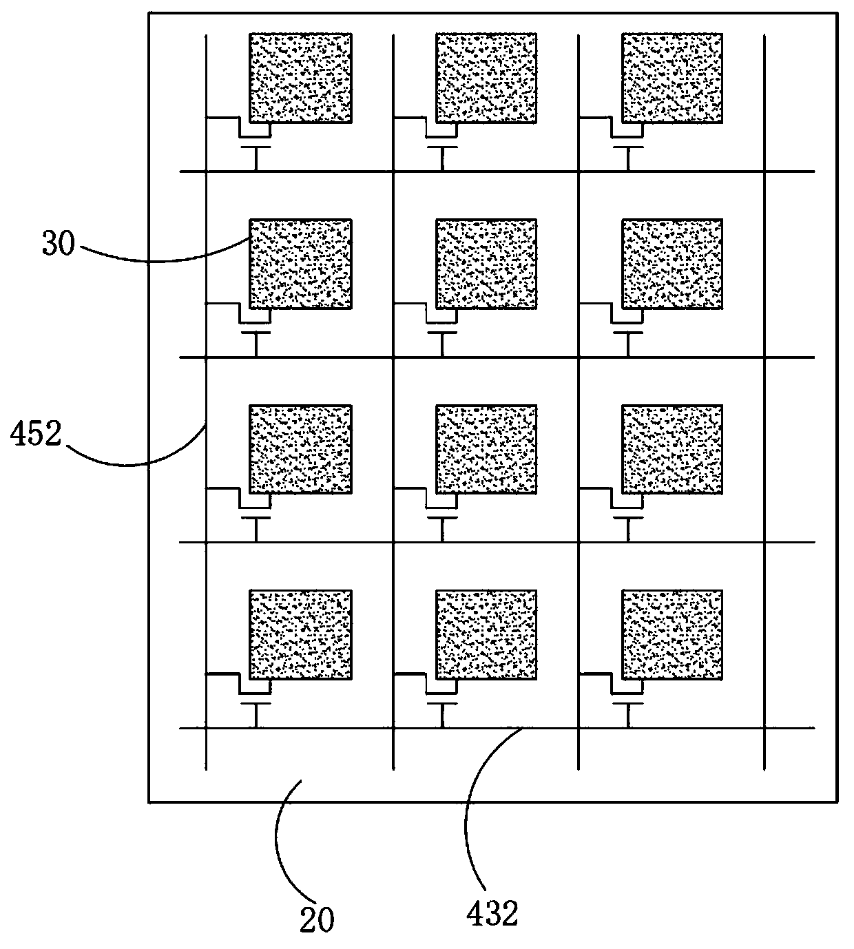
[0045] A display panel such as image 3 As shown, the display panel includes a substrate 20 , a plurality of scan lines 432 disposed on the substrate 20 , a plurality of data lines 452 and a plurality of pixel units 30 arranged in an array on the substrate 20 .
[0046] Specifically, the data lines 452 and the scanning lines 432 are arranged to intersect, the data lines 452 are arranged vertically and a plurality of the data lines 452 are arranged at intervals along the horizontal direction, the scanning lines 432 are arranged horizontally and multiple The scan lines 432 are vertically arranged at intervals, and the area defined by the intersection between two adjacent data lines 452 and two adjacent scan lines 432 is a pixel area where one pixel unit 30 is provided.
[0047] In one embodiment, one scan line 432 corresponds to a row of the pixel units 30 and is electrically connected to provide scan signals for the pixel units 30; one data line 452 corresponds to a column of t...
Embodiment 2
[0078] A display panel such as Figure 10As shown, it differs from Embodiment 1 only in that the position of the distance-increasing surface 384 is different.
[0079] Specifically, the compensation block 38 further includes a second side 382 disposed away from the gap area 32 , and the two opposite edges of the distance-increasing surface 384 are connected to the first side 381 and the second side 382 respectively. .
[0080] Further, the plane where the second side 382 is located is perpendicular to the plane where the first side wall 361 is located, so as to further prevent the first side wall 361 from forming an arc approaching the light-transmitting area 33 during the process of forming the opening 36 .
Embodiment 3
[0082] A display panel such as Figure 11 As shown, the only difference from Embodiment 1 is that the opening 36 also includes a first vertex 364 and a second vertex 365 disposed away from the gap region 32 , the first vertex 364 or / A compensation hole 35 is provided at the second corner 365 , and the compensation hole 35 communicates with the gap region 32 .
[0083] It should be noted that the first vertex 364 and the second vertex 365 are two adjacent corners of the opening 36, and by setting the compensation hole 35 at the corner of the opening 36 away from the gap region 32, the color-resisting block 31 When the opening 36 is formed by laser cutting or etching, the remaining color-resist material can flow into the compensation hole 35 to fill the compensation hole 35, so that the corner of the prepared opening 36 away from the gap region 32 forms a right angle or is close to a right angle, so that the pattern at the corner of the actual opening 36 is closer to the desig...
PUM
 Abstract
Description
Claims
Application Information
 - R&D
- Intellectual Property
- Life Sciences
- Materials
- Tech Scout
- Unparalleled Data Quality
- Higher Quality Content
- 60% Fewer Hallucinations
Browse by: Latest US Patents, China's latest patents, Technical Efficacy Thesaurus, Application Domain, Technology Topic, Popular Technical Reports.
© 2025 PatSnap. All rights reserved.Legal|Privacy policy|Modern Slavery Act Transparency Statement|Sitemap|About US| Contact US: help@patsnap.com