Supercharge Your Innovation With Domain-Expert AI Agents!

Semiconductor device and method for forming same

A semiconductor and device technology, applied in the field of semiconductor devices

Pending Publication Date: 2020-06-26
SK HYNIX INC
View PDF6 Cites 0 Cited by
  • Summary
  • Abstract
  • Description
  • Claims
  • Application Information

AI Technical Summary

Problems solved by technology

[0005] However, the above-mentioned lithography techniques may still have many problems and difficulties in fabricating nanodevices

Method used


Image

  • Semiconductor device and method for forming same
  • Semiconductor device and method for forming same
  • Semiconductor device and method for forming same

Examples


Embodiment Construction

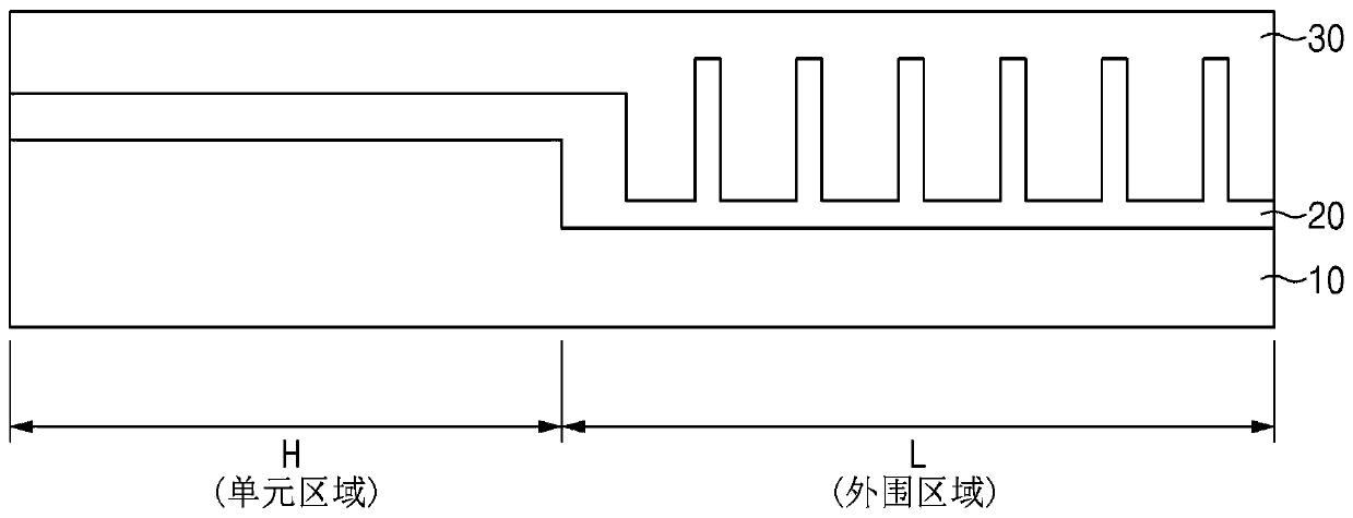
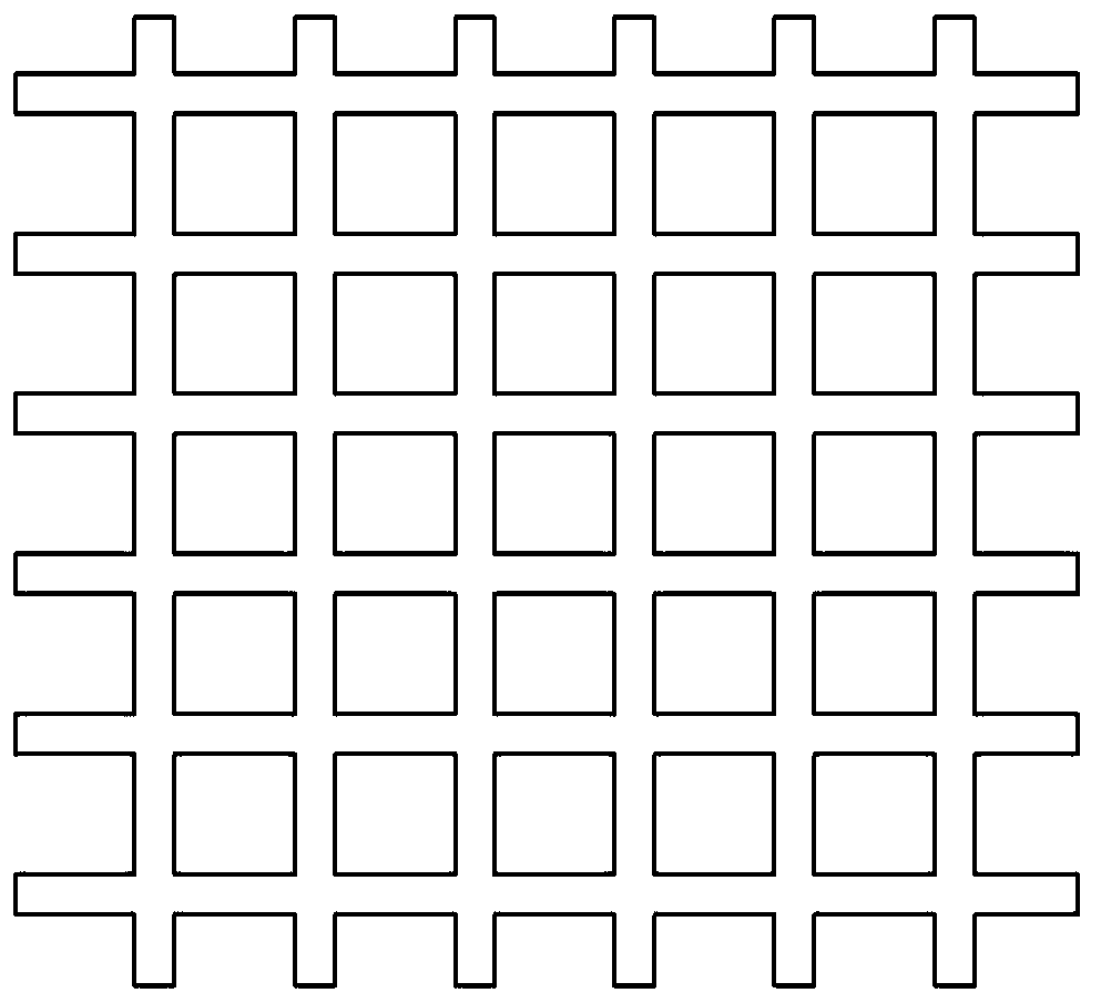
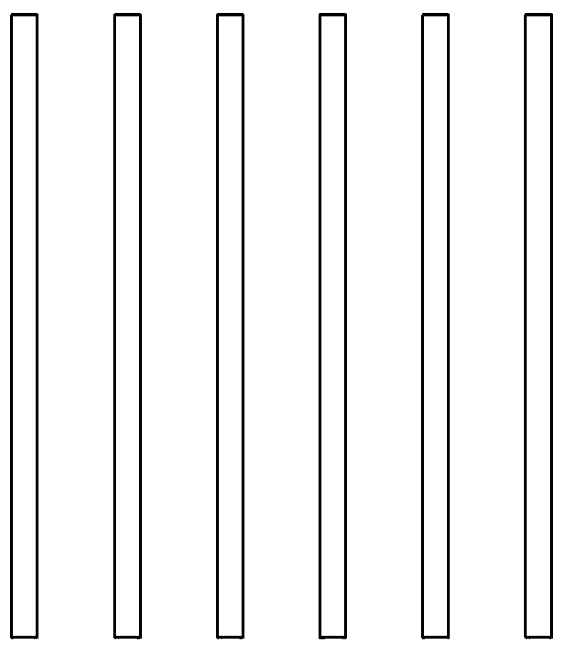
[0018] Various embodiments of the invention are described in more detail below with reference to the accompanying drawings. We note, however, that this invention may be embodied in different forms and modifications and should not be construed as limited to the embodiments set forth herein. Rather, these embodiments are provided so that this disclosure will be thorough and complete, and will fully convey the invention to those of ordinary skill in the art to which this invention pertains. Throughout this disclosure, like reference numerals refer to like parts in the various figures and embodiments of the invention.

[0019] Note that references to "an embodiment," "another embodiment," etc. do not necessarily mean only one embodiment, and that different references to any such phrase do not necessarily refer to the same embodiment.

[0020] It should be understood that although the terms "first," "second," "third," etc. may be used herein to describe various elements, these ele...


PUM

PropertyMeasurementUnit
sizeaaaaaaaaaa

Abstract

A semiconductor device and a method for forming the same are disclosed. The semiconductor device includes a transfer-receiving substrate having a high region and a low region that are different in top-surface height from each other; a transfer-receiving pattern layer formed over the high region and the low region of the transfer-receiving substrate in a manner that a top surface of the transfer-receiving pattern layer in the high region is planarized and a top surface of the transfer-receiving pattern layer in the low region is provided with a concave-convex pattern; and a planarization layerformed to fill the gaps of the concave-convex pattern in a manner that the top surface of the planarization layer in the high region and the top surface of the planarization layer in the low region are planarized at a substantially same level.

Description

technical field [0001] Embodiments of the present disclosure generally relate to semiconductor devices, and more particularly, to a semiconductor device including a planarization layer formed by a spin-coating-based nanoimprint lithography (NIL) technique and a method of forming the semiconductor device. Background technique [0002] Photolithography is a traditional fine structure (microstructure) manufacturing technique used to print and form complex integrated circuit (IC) patterns on semiconductor substrates coated with photoresist films. The size of the formed pattern may be limited by the phenomenon of optical diffraction, and the resolution of the pattern may depend on the thickness of the photoresist film and the wavelength of the light source. Therefore, in general, in order to form fine patterns of smaller size in proportion to the increasing integration of constituent elements of semiconductor devices, an exposure technique based on a short-wavelength light source...

Claims


Application Information

Patent Timeline
Patent Type & Authority Applications(China)
IPC IPC(8): H01L21/027G03F7/00
CPCH01L21/0273G03F7/0002H01L21/76819H01L21/76837H01L21/0274G03F7/0035G03F7/094H10B20/60
Inventor 郑宇荣
Owner SK HYNIX INC
Features
  • R&D
  • Intellectual Property
  • Life Sciences
  • Materials
  • Tech Scout
  • Unparalleled Data Quality
  • Higher Quality Content
  • 60% Fewer Hallucinations
Learn More