Double-sided light-transmitting cadmium telluride solar cell and preparation method thereof
A solar cell, double-sided technology, applied in photovoltaic power generation, circuits, electrical components, etc., can solve the problems of light energy utilization rate, photoelectric conversion rate and low power generation of cadmium telluride solar cells, so as to improve the light energy utilization rate , the method is simple, and the effect of increasing the carrier concentration
- Summary
- Abstract
- Description
- Claims
- Application Information
AI Technical Summary
Problems solved by technology
Method used
Image
Examples
preparation example Construction
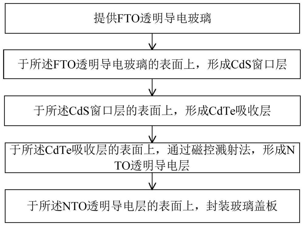
[0045] refer to figure 2 , this embodiment also provides a method for preparing a double-sided light-transmitting CdTe solar cell, comprising the following steps:
[0046] Provide FTO transparent conductive glass 1;
[0047] On the surface of the FTO transparent conductive glass 1, a CdS window layer 2 is formed;
[0048] On the surface of the CdS window layer 2, a CdTe absorbing layer 3 is formed;
[0049] On the surface of the CdTe absorption layer 3, an NTO transparent conductive layer 4 is formed by magnetron sputtering;
[0050] On the surface of the NTO transparent conductive layer 4 , a glass cover plate 5 is encapsulated.
[0051] Specifically, the double-sided light-transmitting CdTe solar cell prepared by this method may include the above-mentioned double-sided light-transmitting CdTe solar cell, but is not limited thereto, and the preparation method of the above-mentioned double-sided light-transmitting CdTe solar cell is not limited to limited to this.
[005...
Embodiment 1
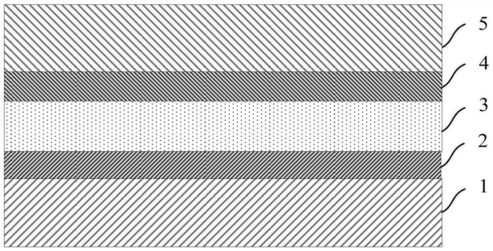
[0057] This embodiment is a double-sided light-transmitting CdTe solar cell, such as figure 1 As shown, it includes: FTO transparent conductive glass 1 , CdS window layer 2 , CdTe absorption layer 3 , NTO transparent conductive layer 4 and glass cover plate 5 from bottom to top.
[0058] The preparation process is as follows:
[0059] a) Provide the FTO transparent conductive glass 1 with a thickness of 3.2 mm, clean it with a brush in deionized water, and dry it with an air knife;
[0060] b) On the cleaned upper surface of the FTO transparent conductive glass 1, a CdS window layer 2 with a thickness of 50 nm is deposited at a deposition temperature of 250° C. by a close-space sublimation method, and deposited at a deposition temperature of 500° C. Under the conditions, a 2 μm thick CdTe absorber layer 3 is deposited.
[0061] c) The sample in the operation b) is taken out, and the NTO transparent conductive layer 4 is deposited by using the magnetron sputtering method, and...
Embodiment 2
[0071] This embodiment provides another preparation method of double-sided light-transmitting CdTe solar cells, such as figure 1 As shown, it includes: FTO transparent conductive glass 1 , CdS window layer 2 , CdTe absorption layer 3 , NTO transparent conductive layer 4 and glass cover plate 5 from bottom to top.
[0072] The preparation process is as follows:
[0073] a) Provide the FTO transparent conductive glass 1 with a thickness of 2.5mm, ultrasonically treat it in absolute alcohol for 10min, and dry it with nitrogen;
[0074] b) On the surface of the cleaned FTO transparent conductive glass 1, a 100nm thick CdS window layer 2 is deposited at a deposition temperature of 300° C. by vapor phase transport method, and deposited at a deposition temperature of 400° C. Under the conditions, a 2 μm thick CdTe absorber layer 3 is deposited.
[0075] c) The sample in the operation b) is taken out, and the NTO transparent conductive layer 4 is deposited by using the magnetron spu...
PUM
| Property | Measurement | Unit |
|---|---|---|
| thickness | aaaaa | aaaaa |
| thickness | aaaaa | aaaaa |
| thickness | aaaaa | aaaaa |
Abstract
Description
Claims
Application Information
 - R&D Engineer
- R&D Manager
- IP Professional
- Industry Leading Data Capabilities
- Powerful AI technology
- Patent DNA Extraction
Browse by: Latest US Patents, China's latest patents, Technical Efficacy Thesaurus, Application Domain, Technology Topic, Popular Technical Reports.
© 2024 PatSnap. All rights reserved.Legal|Privacy policy|Modern Slavery Act Transparency Statement|Sitemap|About US| Contact US: help@patsnap.com


