Manufacturing method of silicon heterojunction solar cell assembly
A solar cell module and silicon heterojunction technology, which is applied in the field of solar cells, can solve the problems of affecting the microstructure of amorphous silicon, deteriorating the passivation effect of heterojunction solar cells, and adversely affecting the conversion efficiency of silicon heterojunction solar cells. , to reduce the production cost, improve the passivation effect, and improve the conversion efficiency.
- Summary
- Abstract
- Description
- Claims
- Application Information
AI Technical Summary
Problems solved by technology
Method used
Image

Examples
Embodiment 1
[0030] This embodiment provides a method for manufacturing a silicon heterojunction solar cell module, comprising the following steps:
[0031] (1) Preparation of silicon heterojunction solar cells;
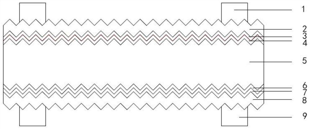
[0032] The silicon heterojunction solar cell includes an N-type silicon heterojunction solar cell on the front side and a P-type silicon heterojunction solar cell on the front side. The back is followed by: front metal grid electrode, transparent conductive oxide (TCO) layer, N-type amorphous silicon layer (n-α-Si:H), intrinsic amorphous silicon layer (i-α-Si:H) , N-type crystalline silicon (C-Si), intrinsic amorphous silicon layer (i-α-Si:H), P-type amorphous silicon layer (p-α-Si:H), transparent conductive oxide (TCO) Layer, back metal grid line electrode; the front side is P-type silicon heterojunction solar cell and the above sequence is reversed, no more details, the cell structure can refer to figure 1 .
[0033] (2) Connect silicon heterojunction solar cells in series a...
Embodiment 2
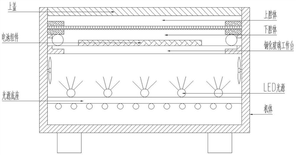
[0042] The difference between this example and Example 1 is that light injection is performed after the preparation of the silicon heterojunction solar cell in step (1), and the light injection is at a temperature of 50-250°C and a light intensity of 0.1-80 solar rays Strong, illumination time 1-600s, light source spectral range 200-2000nm, LED light source adopts one of white light, infrared light and ultraviolet light. This step can improve the passivation effect of the amorphous silicon layer on the amorphous silicon during the preparation process of the solar cell, and improve the conversion efficiency of the solar cell.
Embodiment 3
[0044] The difference between this embodiment and Embodiment 1 is that in the lamination process of the step (4): the lamination heating temperature is controlled at 155° C., the lamination time is 20 minutes, and the light intensity of the LED light source used at the same time is 70 The sunlight is strong, and the LED light source uses infrared light.
PUM
| Property | Measurement | Unit |
|---|---|---|
| Spectral range | aaaaa | aaaaa |
| Thickness | aaaaa | aaaaa |
| Melting point | aaaaa | aaaaa |
Abstract
Description
Claims
Application Information
 - Generate Ideas
- Intellectual Property
- Life Sciences
- Materials
- Tech Scout
- Unparalleled Data Quality
- Higher Quality Content
- 60% Fewer Hallucinations
Browse by: Latest US Patents, China's latest patents, Technical Efficacy Thesaurus, Application Domain, Technology Topic, Popular Technical Reports.
© 2025 PatSnap. All rights reserved.Legal|Privacy policy|Modern Slavery Act Transparency Statement|Sitemap|About US| Contact US: help@patsnap.com