Check patentability & draft patents in minutes with Patsnap Eureka AI!

Manufacturing method of three-dimensional memory and three-dimensional memory

A manufacturing method and memory technology, which are applied to semiconductor devices, electric solid-state devices, semiconductor/solid-state device components, etc., can solve problems such as damage to the control circuit structure and decrease in the reliability of three-dimensional memory, reduce static electricity, and enhance the effect of sharing and drainage. , the effect of enhancing structural stability and reliability

Active Publication Date: 2021-09-28
YANGTZE MEMORY TECH CO LTD
View PDF5 Cites 0 Cited by
  • Summary
  • Abstract
  • Description
  • Claims
  • Application Information

AI Technical Summary

Problems solved by technology

[0003] However, in the current manufacturing method of three-dimensional memory, after the array chip and the circuit chip are bonded, it is necessary to etch the substrate of the array chip to extract the metal interconnection structure from the back of the array chip, which requires the use of plasma Etching and deposition processes, among which, plasma etched ions carry a lot of static electricity, which will be transmitted to each control circuit in the circuit chip along the metal interconnection structure, causing damage to the structure of the control circuit, resulting in three-dimensional memory drop in reliability

Method used


Image

  • Manufacturing method of three-dimensional memory and three-dimensional memory
  • Manufacturing method of three-dimensional memory and three-dimensional memory
  • Manufacturing method of three-dimensional memory and three-dimensional memory

Examples


Embodiment Construction

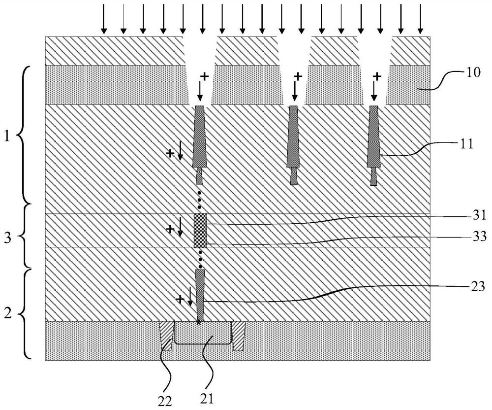
[0041] The inventor found that in the current manufacturing process of the three-dimensional memory, such as figure 1 As shown, after the array chip (i.e. storage array wafer) 1 and the circuit chip (i.e. CMOS circuit wafer) 2 are bonded through the bonding connection part 3, it is also necessary to etch the base 10 of the array chip 1, and the first metal The contact structure 11 is drawn out from the back of the array chip 1, which requires plasma etching, and the ions of plasma etching carry static electricity ( figure 1 middle "+" sign), static electricity will be conducted to the control circuit 21 on the circuit chip 2 along the first metal contact structure 11, the first pad 31, the third pad 33 and the second metal contact structure 23, a large amount of The accumulation of static electricity will cause structural damage to the control circuit 21, resulting in a decrease in the reliability of the three-dimensional memory.

[0042]Therefore, the present invention propo...


PUM


Abstract

The present invention provides a method for manufacturing a three-dimensional memory and a three-dimensional memory. In the method for manufacturing a three-dimensional memory, a plurality of first dummy metal contact structures are formed around the first metal contact structure in an array chip, so that subsequent The static electricity caused by etching is shared and drained; in addition, in the circuit chip, a static elimination circuit electrically connected with the first dummy metal contact structure is added, so that the static electricity elimination circuit can capture or eliminate the static electricity accumulated on the first dummy metal contact structure. Static electricity, further strengthen the sharing and drainage effect of static electricity, so that the amount of static electricity transmitted to the control circuit on the circuit chip through the first metal contact structure and the second metal contact structure can be greatly reduced, and the static electricity caused by etching can be effectively avoided. The damage of the circuit chip enhances the structural stability and reliability of the control circuit on the circuit chip.

Description

technical field [0001] The invention relates to the technical field of semiconductor manufacturing, in particular to a manufacturing method of a three-dimensional memory and a three-dimensional memory. Background technique [0002] Three-dimensional memory is a technology for stacking data units. At present, data units of 32 layers and above can be stacked. It overcomes the limitation of the actual expansion limit of planar memory, further increases the storage capacity, and reduces the storage cost of each data bit. , reducing energy consumption. [0003] However, in the current manufacturing method of three-dimensional memory, after the array chip and the circuit chip are bonded, it is necessary to etch the substrate of the array chip to extract the metal interconnection structure from the back of the array chip, which requires the use of plasma Etching and deposition processes, among which, plasma etched ions carry a lot of static electricity, which will be transmitted t...

Claims


Application Information

Patent Timeline
Patent Type & Authority Patents(China)
IPC IPC(8): H01L27/11521H01L27/11551H01L27/11568H01L27/11578H01L23/60H01L27/02H10B41/30H10B41/20H10B43/20H10B43/30
CPCH01L27/0296H01L23/60H10B41/30H10B41/20H10B43/30H10B43/20
Inventor 彭进霍宗亮董金文华子群
Owner YANGTZE MEMORY TECH CO LTD
Features
  • R&D
  • Intellectual Property
  • Life Sciences
  • Materials
  • Tech Scout
  • Unparalleled Data Quality
  • Higher Quality Content
  • 60% Fewer Hallucinations
Learn More