

N-type AlN ohmic contact structure, AlN Schottky diode and AlN field effect transistor
A technology of field-effect transistors and ohmic contact electrodes, which is applied in the field of semiconductor devices, can solve problems such as difficulty in realizing electron diffusion, drift and tunneling, high ionization energy of doped impurities, and difficulty in achieving heavy doping.
- Summary
- Abstract
- Description
- Claims
- Application Information
AI Technical Summary
Problems solved by technology
Method used
Image


Examples
Embodiment 1
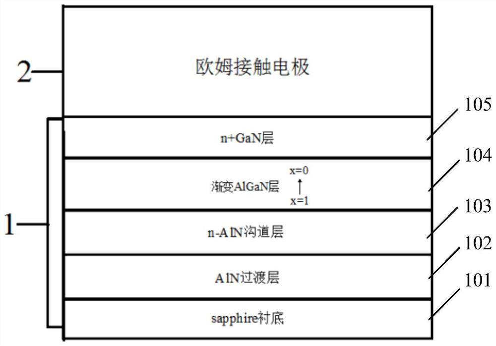
[0033] figure 1 It is a structural schematic diagram of an n-type AlN ohmic contact structure provided by an embodiment of the present invention. The structure includes a wafer structure 1 and an ohmic contact electrode 2 , and the ohmic contact electrode 2 is arranged on the wafer structure 1 . The wafer structure 1 includes a substrate layer 101 , a transition layer 102 , a channel layer 103 , a graded AlGaN layer 104 and an n-type GaN layer 105 arranged sequentially from bottom to top. The material of the substrate layer 101 is sapphire (sapphire), which is 2 inches; the material of the transition layer 102 is AlN, and the thickness is 4 μm; the material of the channel layer 103 is AlN, and the thickness is 500 nm. The doping type is n-type, and the doping concentration 1×10 16; The content of the Al component in the graded AlGaN layer 104 gradually changes from 1 to 0 from bottom to top, the thickness is 100nm, the doping type is n-type, and the doping concentration is 1...
Embodiment 2
[0041] Based on the first embodiment, this embodiment provides an AlN Schottky diode. See figure 2 , figure 2 It is a schematic structural diagram of an AlN Schottky diode provided by an embodiment of the present invention. The AlN Schottky diode includes a wafer structure 1 , an anode 4 and a cathode 3 . The wafer structure 1 includes a substrate layer 101 , a transition layer 102 , a channel layer 103 , a graded AlGaN layer 104 and an n-type GaN layer 105 arranged sequentially from bottom to top. The cathode 3 covers the upper surface of the n-type GaN layer 105, and a part of the upper surface of the channel layer 103 covers the graded AlGaN layer 104, so that the anode 4 is also arranged on the upper surface of the channel layer 103, and the anode 4 and the graded AlGaN layer 104 does not touch.
[0042] Preferably, the cathode 3 is composed of four layers of metal materials, the four layers of materials are titanium, aluminum, nickel, and gold from bottom to top, an...
Embodiment 3
[0050] Based on the above embodiments, this embodiment provides an AlN Schottky gate field effect transistor. See Figure 4 , Figure 4 It is a schematic structural diagram of an AlN Schottky gate field effect transistor provided by an embodiment of the present invention. The AlN Schottky gate field effect transistor includes a wafer structure 1, a source 5, a drain 6, and a gate 7, wherein the wafer structure 1 includes a substrate layer 101, a transition layer 102, and a trench arranged sequentially from bottom to top. layer 103, graded AlGaN layer 104 and n-type GaN layer 105. The source 5 and the drain 6 are respectively located on both sides of the upper surface of the n-type GaN layer 105 , and the gate 7 is located on the upper surface of the channel layer 103 .
[0051] Preferably, the source electrode 5 is composed of four layers of metal materials, the four layers of materials are titanium / aluminum / nickel / gold from bottom to top, and the thicknesses are 22 / 140 / 45 / ...
PUM
| Property | Measurement | Unit |
|---|---|---|
| Thickness | aaaaa | aaaaa |
| Thickness | aaaaa | aaaaa |
| Thickness | aaaaa | aaaaa |
Abstract
Description
Claims
Application Information