
Photomask

A photomask and light blocking technology, applied in the field of photomasks, can solve problems such as affecting metal rewiring, reducing the pass rate of chip products, and metal rewiring disconnection.

Pending Publication Date: 2021-04-27
苏州科阳半导体有限公司
View PDF0 Cites 0 Cited by
  • Summary
  • Abstract
  • Description
  • Claims
  • Application Information

AI Technical Summary

Problems solved by technology

The too thick photoresist at the lower corner 102 increases the width of the metal rewiring and connects with other lines, resulting in a short circuit. In order to ensure that the thicker photoresist layer at the lower corner 102 can be formed by photolithography The metal rewiring of the pattern is usually selected with a larger exposure energy during photolithography, and because the photoresist layer at the upper corner 101 is too thin, the excessive exposure energy leads to severe overexposure at the upper corner 101, making the metal heavy In the case of open circuit in the wiring, the above two situations affect the function of metal rewiring and reduce the qualified rate of chip products
The light-blocking pattern on the photomask in the prior art is difficult to obtain metal rewiring without short circuit and open circuit on the chip with etched groove 100

Method used


Image

  • Photomask
  • Photomask

Examples


Embodiment Construction

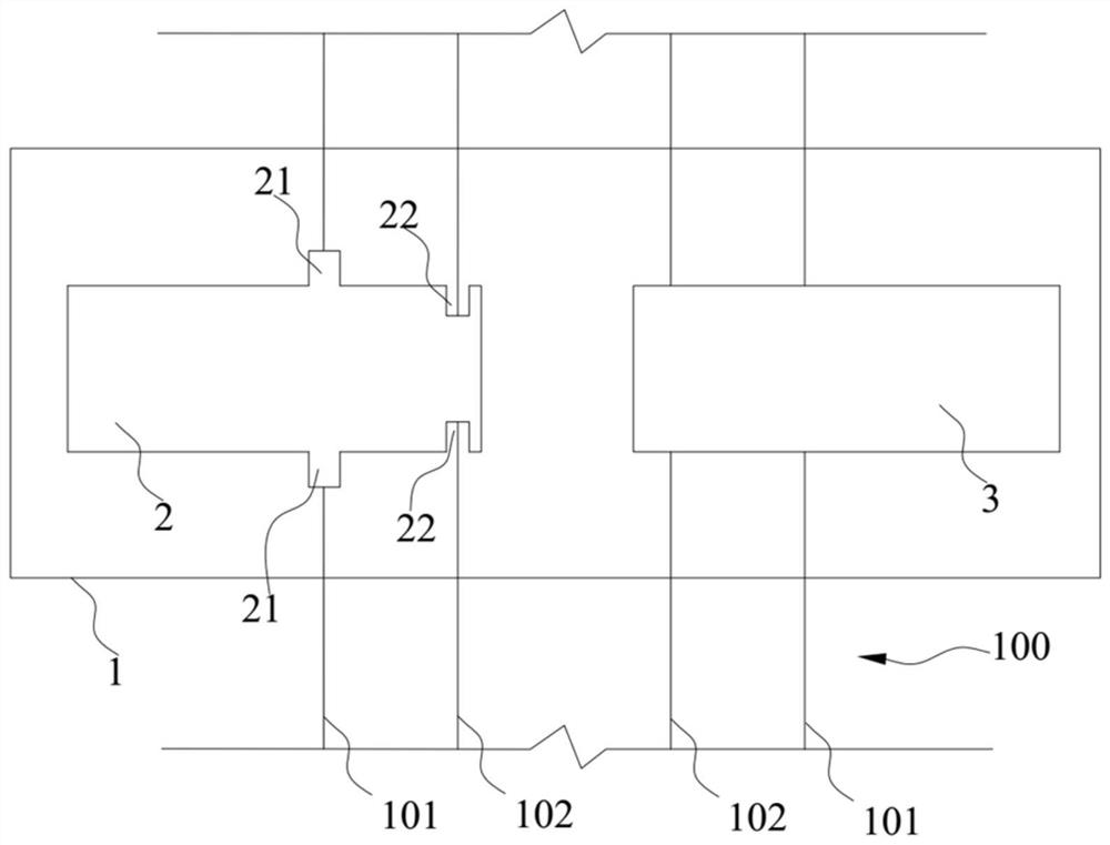
[0024] In order to make the technical problems solved by the present invention, the technical solutions adopted and the technical effects achieved clearer, the technical solutions of the embodiments of the present invention will be further described in detail below in conjunction with the accompanying drawings. Obviously, the described embodiments are only the technical solutions of the present invention. Some, but not all, embodiments. Based on the embodiments of the present invention, all other embodiments obtained by those skilled in the art without making creative efforts belong to the protection scope of the present invention.

[0025] In the description of the present invention, unless otherwise clearly specified and limited, the terms "connected", "connected" and "fixed" should be understood in a broad sense, for example, it can be a fixed connection, a detachable connection, or an integrated ; It can be a mechanical connection or an electrical connection; it can be a d...


PUM

PropertyMeasurementUnit
Lengthaaaaaaaaaa

Abstract

The invention relates to the technical field of semiconductor manufacturing, and discloses a photomask. The photomask is used for forming metal redistribution lines at an etching groove through photoetching, the etching groove comprises an upper corner located at the top of the groove and a lower corner located at the bottom of the groove, and the etching groove extends in the first direction of the horizontal plane. The photomask comprises a transparent substrate and a light blocking pattern. The light blocking pattern is arranged on the transparent substrate and can block laser beams or ultraviolet light from penetrating through the transparent substrate, the light blocking pattern comprises a first light blocking area extending in the second direction on the horizontal plane, the first direction is perpendicular to the second direction, the first light blocking area is provided with a widened part and a concave part, the widened part is arranged on the edge of the first light blocking area in a protruding mode, the concave part is concavely arranged at the edge of the first light blocking area, the projection of the widened part on the etching groove is at the upper corner, and the projection of the concave part on the etching groove is at the lower corner. According to the invention, the possibility of short circuit or open circuit of the redistribution line at the etching groove is reduced, the function of the redistribution line is ensured, and the percent of pass of products is improved.

Description

technical field [0001] The invention relates to the technical field of semiconductor manufacturing, in particular to a photomask. Background technique [0002] On a semiconductor chip, metal rewiring is generally provided for the convenience of wiring. Now the passivation layer is laid on the wafer, a layer of metal is sputtered on the passivation layer, and then a layer of photoresist is sprayed or spin-coated on the metal layer, and then irradiated by laser or ultraviolet light through the photolithography process. The remaining metal area is finally developed to obtain the required rewiring pattern. A photomask is used to assist in photolithography. The photomask includes a transparent substrate, and the transparent substrate is provided with a light-blocking pattern that can form a preset metal rewiring pattern. The light-blocking pattern can prevent the laser beam from passing through the transparent substrate. During photolithography, the photomask is placed above th...

Claims


Application Information

Patent Timeline
IPC IPC(8): G03F1/38
CPCG03F1/38
Inventor 杨鹏陈胜江勇顾浩宇
Owner 苏州科阳半导体有限公司
Features
  • Generate Ideas
  • Intellectual Property
  • Life Sciences
  • Materials
  • Tech Scout
  • Unparalleled Data Quality
  • Higher Quality Content
  • 60% Fewer Hallucinations
Learn More