

Resistive random access memory array and manufacturing method thereof
A technology of resistive random access memory, applied in the direction of electric solid devices, circuits, electrical components, etc., can solve the problems of increasing process complexity, production time and production cost, complex circuit design, occupation, etc., to increase the operating window. The effect of chaos and complexity reduction
- Summary
- Abstract
- Description
- Claims
- Application Information
AI Technical Summary
Problems solved by technology
Method used
Image


Examples
Embodiment Construction
[0027] In order to make the purpose, features and advantages of the present invention more comprehensible, preferred embodiments are listed below and described in detail in conjunction with the accompanying drawings.
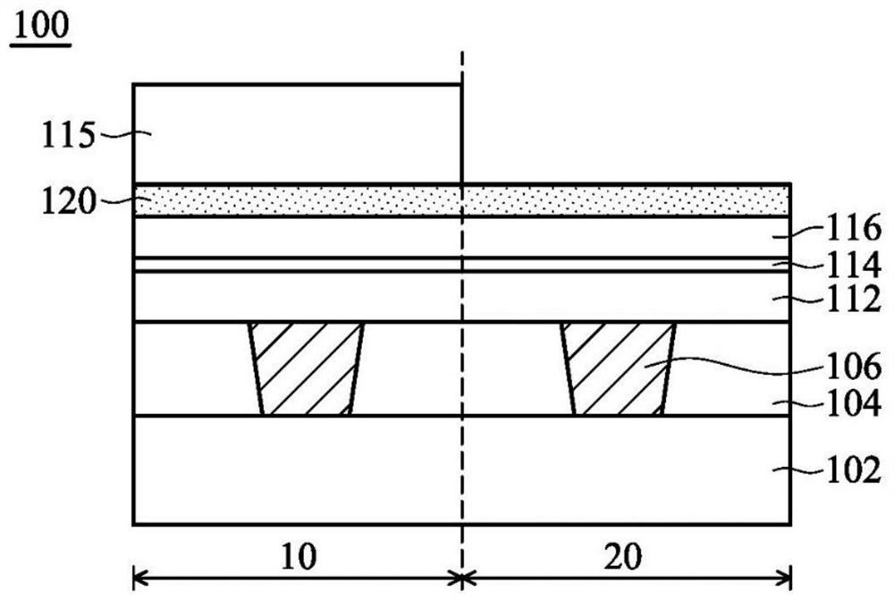
[0028] Figure 1A to Figure 1F It is a schematic cross-sectional view corresponding to each step of the manufacturing method of the resistive random access memory array 100 in some embodiments of the present invention. Please refer to Figure 1A , a substrate 102 is provided, and the array area of the substrate 102 includes a first area 10 and a second area 20 . Next, an insulating layer 104 is formed on the substrate 102 . Materials of the substrate 102 may include bulk semiconductor substrates (eg, silicon substrates), compound semiconductor substrates (eg, Group IIIA-VA semiconductor substrates), silicon-on-insulator (SOI) substrates, and the like. The substrate 102 can be a doped or undoped semiconductor substrate. In some embodiments, substrate 102 is ...
PUM
 Abstract
Description
Claims
Application Information