MEMS capacitive pressure sensor chip and manufacturing process thereof
A pressure sensor and capacitive technology, which is applied in the direction of fluid pressure measurement, instrument, and measuring force using capacitance changes, can solve the structure damage of movable plates, the difficulty of eliminating coupling capacitance interference, and the poor environmental adaptability of MEMS capacitive pressure sensors and other issues, to achieve the effect of isolating external electromagnetic interference, strong environmental adaptability, and eliminating the proportion of capacitance
- Summary
- Abstract
- Description
- Claims
- Application Information
AI Technical Summary
Problems solved by technology
Method used
Image
Examples
Embodiment 1
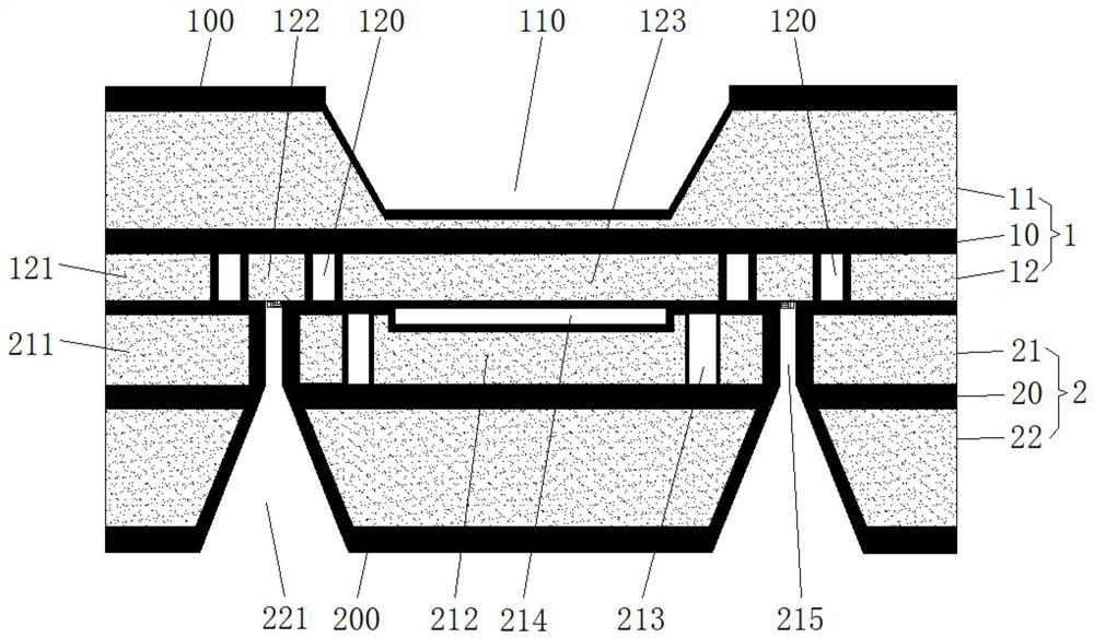
[0051] Such as Figure 1-6 As shown, a MEMS capacitive pressure sensor chip includes:
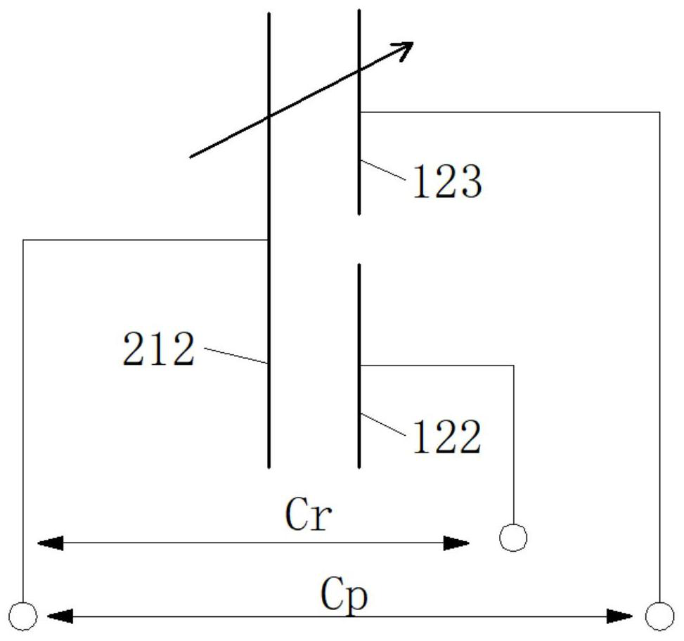
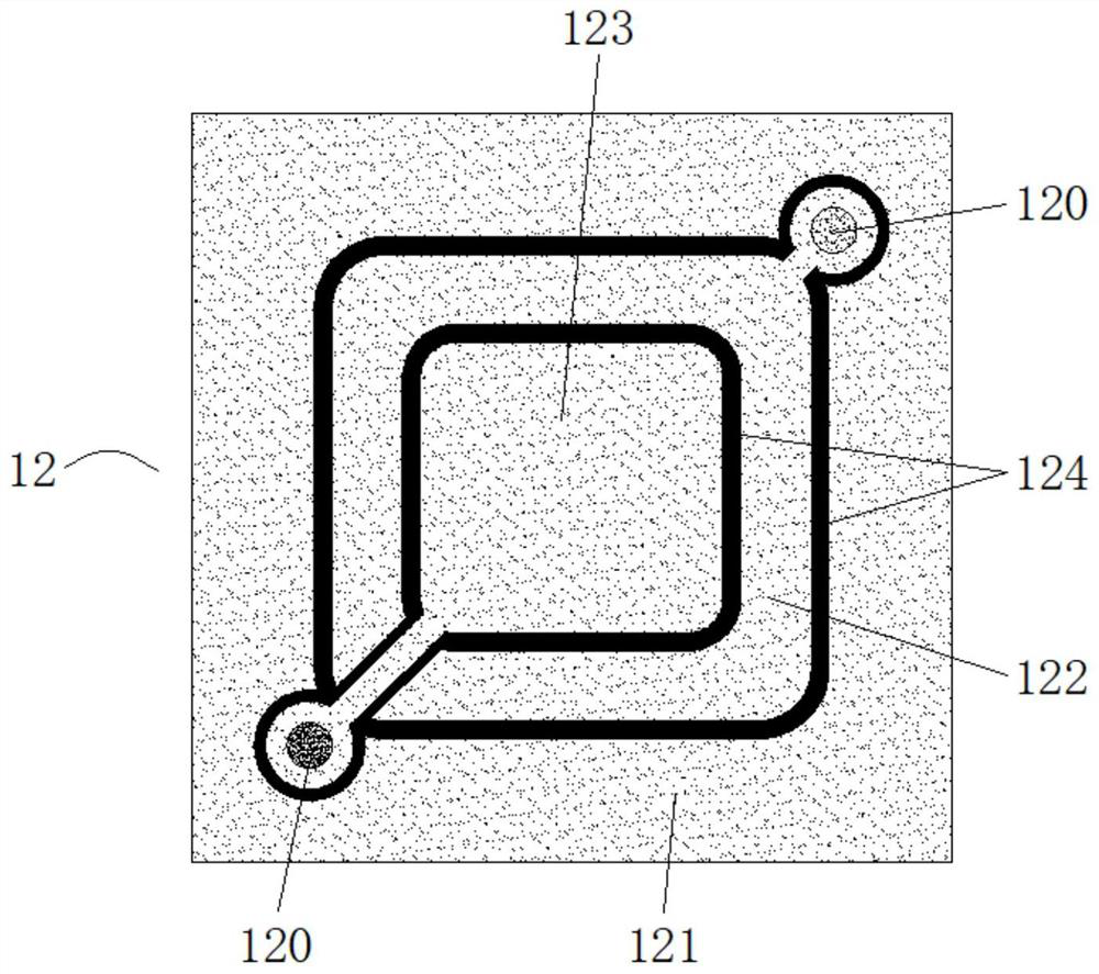
[0052] The first wafer 1 includes a first structural layer 11 and a movable electrode layer 12 that are bonded to each other, and a first insulating layer 10 is disposed between the first structural layer 11 and the movable electrode layer 12 . The movable electrode layer 12 penetrates through the overall etching to form the first closed ring 121, the reference capacitor plate 122 and the movable capacitor plate 123 which are physically and electrically isolated from each other. The first closed ring 121, the reference capacitor plate 122 and the movable The capacitor plates 123 are separated from each other by two first isolation grooves 124 . The reference capacitor plate 122 and the movable capacitor plate 123 are respectively provided with a first contact electrode 120, the top of the first structure layer 11 is provided with a cavity 110 that does not penetrate the first structure lay...
Embodiment 2
[0071] Such as Figure 8 As shown, the structure and working principle of the MEMS capacitive pressure sensor chip of this embodiment are all the same as that of Embodiment 1, and the manufacturing process of this embodiment includes the following steps:
[0072] Prepare SOI wafers, Si wafers and glass wafers respectively. Due to the unique three-layer structure of SOI wafers, use the three-layer structure of SOI wafers to make the first structure layer 11, the movable electrode layer 12 and the first insulating layer. 10. Fabricate the fixed electrode layer 21 with a Si wafer, and fabricate the second structural layer 22 with a glass wafer.
[0073] The first step is to form a cavity 110 on the SOI wafer that does not penetrate the top layer of the SOI wafer through a wet etching process;
[0074] The second step is to etch through the movable electrode layer 12 on the movable electrode layer 12 of the SOI wafer through a dry etching process to form a first closed ring 121, ...
PUM
| Property | Measurement | Unit |
|---|---|---|
| depth | aaaaa | aaaaa |
Abstract
Description
Claims
Application Information
 - R&D Engineer
- R&D Manager
- IP Professional
- Industry Leading Data Capabilities
- Powerful AI technology
- Patent DNA Extraction
Browse by: Latest US Patents, China's latest patents, Technical Efficacy Thesaurus, Application Domain, Technology Topic, Popular Technical Reports.
© 2024 PatSnap. All rights reserved.Legal|Privacy policy|Modern Slavery Act Transparency Statement|Sitemap|About US| Contact US: help@patsnap.com


