

Manufacturing method of memory device
A manufacturing method and storage device technology, which is applied in semiconductor/solid-state device manufacturing, electrical components, circuits, etc., can solve the problems that the yield rate of storage devices needs to be improved, and achieve the effects of excellent collapse resistance, quality improvement, and performance improvement
- Summary
- Abstract
- Description
- Claims
- Application Information
AI Technical Summary
Problems solved by technology
Method used
Image


Examples
Embodiment Construction
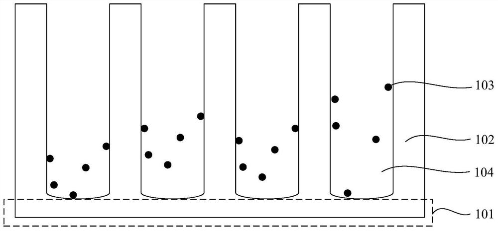
[0025] It can be seen from the background art that the product yield of existing memory devices still needs to be improved. figure 1 and figure 2 It is a structural schematic diagram corresponding to each step of a manufacturing method of a storage device, combined with figure 1 and figure 2 , and analyze the manufacturing method of the memory device:
[0026] refer to figure 1 , providing a base 101 and a protruding portion 102 on the base 101 , and adjacent protruding portions 102 and the base 101 form a groove 104 .
[0027] The process steps of forming the protruding portion 102 generally include a dry etching step and a step of removing the mask layer, resulting in impurities 103 on the surface of the trench 104 .
[0028] refer to figure 2 , using wet cleaning treatment to remove impurities 103 .
[0029] The wet cleaning process includes: in the groove 104 (reference figure 1 ) into the cleaning solution 105 for absorbing or dissolving the impurities 103; dryi...
PUM
| Property | Measurement | Unit |
|---|---|---|
| Thickness | aaaaa | aaaaa |
Abstract
Description
Claims
Application Information