Supercharge Your Innovation With Domain-Expert AI Agents!

Fan-out chip stacking packaging structure and manufacturing method thereof

A packaging structure and chip stacking technology, which is applied in semiconductor/solid-state device manufacturing, semiconductor/solid-state device components, semiconductor devices, etc., can solve the problems of increased resistance, long production cycle, and increased cost, and reduce parasitic resistance and inductance. , the effect of improving high frequency performance and increasing transmission speed

Active Publication Date: 2021-06-15
YANGTZE MEMORY TECH CO LTD
View PDF12 Cites 0 Cited by
  • Summary
  • Abstract
  • Description
  • Claims
  • Application Information

AI Technical Summary

Problems solved by technology

For example, when the wire bonding process is used for packaging, the existence of gold fingers will expand the area of ​​the entire package structure by more than 20%, and the conductive path of the gold wire process is relatively long, which limits the high-frequency performance of the chipset
In addition, due to the longer production cycle required for packaging using the wire bonding process, more wire bonding machines are required to produce a certain number of packaging structures
Due to the limitation of the wiring method, the chips inside the package structure can only lead out the I / O terminals in a single row, which is not conducive to subsequent wiring operations
However, when the TSV process is used for packaging, the cooperation of chip design and chip packaging is required, which is technically difficult and the cost is relatively high.
Since the substrate in the package structure needs to have ultra-small pitch line width / spacing, the manufacturing cost will increase exponentially with the reduction of line width / spacing, and holes need to be drilled during the substrate manufacturing process, and these holes will be used in subsequent manufacturing. The process will not be filled with metal, which will increase a certain resistance, which will affect the high frequency performance of the product

Method used


Image

  • Fan-out chip stacking packaging structure and manufacturing method thereof
  • Fan-out chip stacking packaging structure and manufacturing method thereof
  • Fan-out chip stacking packaging structure and manufacturing method thereof

Examples


Embodiment Construction

[0059] For a better understanding of the application, various aspects of the application will be described in more detail with reference to the accompanying drawings. It should be understood that these detailed descriptions are descriptions of exemplary embodiments of the application only, and are not intended to limit the scope of the application in any way. Throughout the specification, the same reference numerals refer to the same elements. The expression "and / or" includes any and all combinations of one or more of the associated listed items.

[0060] It should be noted that in this specification, expressions of first, second, third, etc. are only used to distinguish one feature from another, and do not represent any limitation on the features. Accordingly, a first electrode discussed hereinafter may also be referred to as a second electrode without departing from the teachings of the present application. vice versa.

[0061] In the drawings, the thickness, size and sha...


PUM


Abstract

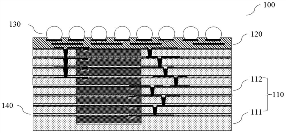
The invention provides a fan-out chip stacking packaging structure and a manufacturing method thereof. The fan-out chip stacking packaging structure comprises a stacking structure, a rewiring structure and a plurality of bump structures. The stacking structure comprises a plurality of stacking units which are stacked in sequence, the rewiring structure is arranged on one surface of the stacking structure, and the plurality of bump structures are arranged on the surface of one side, far away from the stacking units, of the rewiring structure. In one embodiment, chips disposed within the stacking units may have a plurality of rows of I / O ports, which are electrically connected to the plurality of bump structures through the rewiring structure.

Description

technical field [0001] The invention relates to a packaging structure. Specifically, it relates to a fan-out chip stack package structure and a manufacturing method thereof. Background technique [0002] At present, with the maturity of technology in the memory industry, the miniaturization of the memory package structure has become a major development trend. Since the characteristic size of the chip unit inside the package structure is gradually approaching the lower limit, in order to realize the miniaturization of the package structure, the requirements for the chip package technology are getting higher and higher. [0003] In the chip stacking packaging process in the prior art, the wire bonding process and the Through Silicon Via (TSV) process are mainly used, but in the face of the miniaturization requirements, these two packaging processes have some problems that need to be solved urgently . For example, when the wire bonding process is used for packaging, the pres...

Claims


Application Information

Patent Timeline
Patent Type & Authority Applications(China)
IPC IPC(8): H01L23/488H01L25/065H01L21/98
CPCH01L24/02H01L24/03H01L24/11H01L24/14H01L25/0657H01L25/50H01L2224/02379H01L2224/02331H01L2224/0237H01L2224/0231H01L2224/1412
Inventor 曾心如陈鹏周厚德
Owner YANGTZE MEMORY TECH CO LTD
Features
  • R&D
  • Intellectual Property
  • Life Sciences
  • Materials
  • Tech Scout
  • Unparalleled Data Quality
  • Higher Quality Content
  • 60% Fewer Hallucinations
Learn More