Check patentability & draft patents in minutes with Patsnap Eureka AI!

Epitaxial structure and light emitting diode

An epitaxial structure, peak shape technology, applied in semiconductor devices, electrical components, circuits, etc., can solve the problems of reducing the antistatic ability of epitaxial structures, polarization effect dislocation defects, etc., to reduce the risk of electrostatic breakdown, improve The effect of antistatic ability

Active Publication Date: 2021-11-16
XIAMEN SANAN OPTOELECTRONICS CO LTD
View PDF16 Cites 0 Cited by
  • Summary
  • Abstract
  • Description
  • Claims
  • Application Information

AI Technical Summary

Problems solved by technology

The epitaxial structure in GaN-based light-emitting diodes includes an n-type GaN layer, an active layer and a p-type GaN layer, wherein the active layer is a periodic structure composed of alternating GaN layers and InGaN (indium gallium nitride) layers. The lattice constants of the InGaN layer and the InGaN layer are different, and it is easy to produce polarization effects and cause dislocation defects. If the dislocation defects are not effectively controlled, a large number of surface defects will be formed. At the same time, the InGaN layer has a high In concentration, which requires Low temperature growth, surface defects are also formed during the low temperature growth process, these surface defects will form leakage channels and reduce the antistatic ability of the epitaxial structure

Method used


Image

  • Epitaxial structure and light emitting diode
  • Epitaxial structure and light emitting diode

Examples


Embodiment Construction

[0031] The implementation of the present application is described below through specific specific examples, and those skilled in the art can easily understand other advantages and effects of the present application from the content disclosed in this specification. The present application can also be implemented or operated through other different specific implementation modes, and various modifications or changes can be made to the details in the present application based on different viewpoints and applications without departing from the spirit of the present application.

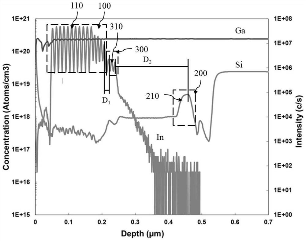
[0032] The composition of each layer included in this application can be analyzed by any suitable means, such as secondary ion mass spectrometry (SIMS); the thickness of each layer can be analyzed by any suitable means, such as transmission electron microscopy (TEM) or scanning Electron Microscopy (SEM) for coordinating, for example, the depth position of each layer on a SIMS map.

[0033] According to one...


PUM

PropertyMeasurementUnit
Doping concentrationaaaaaaaaaa
Thicknessaaaaaaaaaa
Thicknessaaaaaaaaaa

Abstract

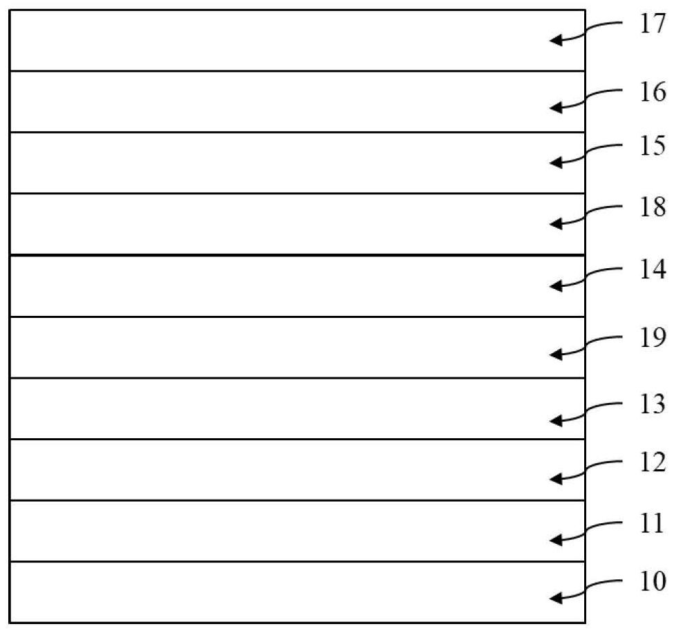
The invention discloses an epitaxial structure and a light emitting diode. Theepitaxial structure comprises an n-type layer, a p-type layer and an active layer, wherein the active layer comprising a first concentration profile of In having a first peak shape; a heavily doped layer which is positioned between the n-type layer and the active layer and comprises a second concentration profile of Si with a second peak shape; and a current expansion layer which is positioned between the heavily doped layer and the active layer and comprises a third concentration profile of In with a third peak shape. The minimum distance between the peak top of the third peak shape and the peak top of the first peak shape is D1, the minimum distance between the peak top of the third peak shape and the peak top of the second peak shape is D2, and the ratio of D1 to D2 is smaller than 1: 7. The current expansion layer is close to the active layer as much as possible and effectively guides impact current when subjected to electrostatic impact, so that the active layer is protected from being easily broken down by static electricity; meanwhile, the area between the current expansion layer and the heavily doped layer is an electronic storage area, the risk that the epitaxial structure is broken down by static electricity can be reduced when the epitaxial structure is impacted by static electricity, and therefore the anti-static electricity capacity of the epitaxial structure and the light-emitting diode is improved.

Description

technical field [0001] The present application relates to the technical field related to semiconductors, in particular to an epitaxial structure and a light emitting diode. Background technique [0002] Group III nitrides represented by gallium nitride (GaN) are direct transition wide bandgap semiconductor materials, which have high thermal conductivity, high hardness, small dielectric constant, high temperature resistance, acid and alkali resistance, etc., and are widely used in Blue light, green light, ultraviolet light-emitting diodes. The epitaxial structure in GaN-based light-emitting diodes includes an n-type GaN layer, an active layer and a p-type GaN layer, wherein the active layer is a periodic structure composed of alternating GaN layers and InGaN (indium gallium nitride) layers. The lattice constants of the InGaN layer and the InGaN layer are different, and it is easy to produce polarization effects and cause dislocation defects. If the dislocation defects are no...

Claims


Application Information

Patent Timeline
IPC IPC(8): H01L33/04H01L33/06H01L33/14H01L33/32
CPCH01L33/04H01L33/06H01L33/14H01L33/325H01L33/0075
Inventor 叶大千
Owner XIAMEN SANAN OPTOELECTRONICS CO LTD
Features
  • R&D
  • Intellectual Property
  • Life Sciences
  • Materials
  • Tech Scout
  • Unparalleled Data Quality
  • Higher Quality Content
  • 60% Fewer Hallucinations
Learn More