Power semiconductor module
A technology of semiconductor and electric power, which is applied in the direction of semiconductor devices, semiconductor/solid-state device components, electric solid-state devices, etc., can solve the problems of current unbalance, unable to suppress current unbalance, etc., and achieve the effect of suppressing current unbalance
- Summary
- Abstract
- Description
- Claims
- Application Information
AI Technical Summary
Problems solved by technology
Method used
Image
Examples
Embodiment approach 1
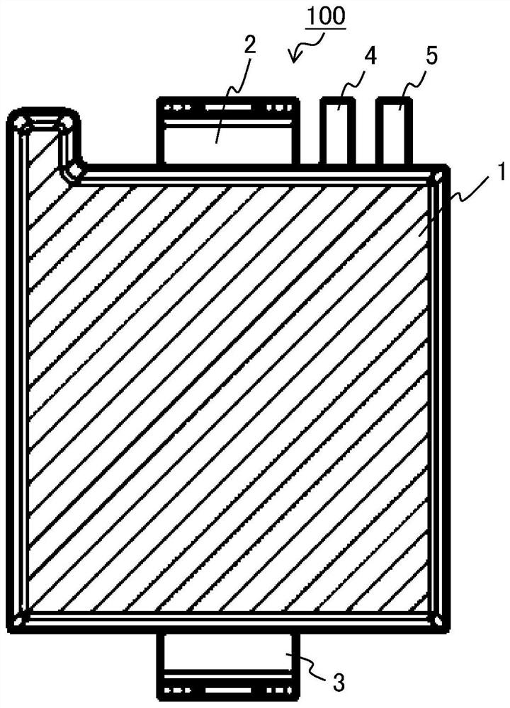
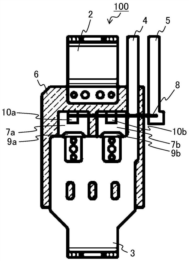
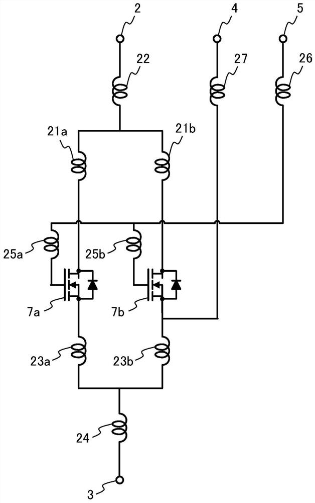
[0053] figure 1 It is a figure showing the appearance of the power semiconductor module 100 according to the first embodiment. figure 2It is a diagram showing the internal structure of the power semiconductor module 100 according to Embodiment 1, except for the resin module 1 . The power semiconductor module 100 according to Embodiment 1 includes a resin mold 1, a P bus bar 2, an N bus bar 3, a control ground terminal 4, a control gate terminal 5, a heat-dissipating metal substrate 6, a semiconductor switching element 7a, a semiconductor Switching element 7 b and bonding wire 8 . The semiconductor switching element 7a includes a source electrode 9a and a gate pad 10a on the front surface, and a drain electrode (not shown) on the back surface. The semiconductor switching element 7b includes a source electrode 9b and a gate pad 10b on the front surface, and a drain electrode (not shown) on the back surface. A semiconductor switching element 7 a and a semiconductor switching ...
Embodiment approach 2
[0070] Figure 4 It is a figure showing the appearance of the power semiconductor module 200 according to the second embodiment. Figure 5 It is a figure which shows the internal structure of the semiconductor module 200 for electric power of Embodiment 2 except the resin module 1a. The power semiconductor module 200 according to the second embodiment is based on a configuration in which the power semiconductor module 100 according to the first embodiment is mirror-symmetrically arranged with the reference line 1000 as the axis of symmetry.
[0071] The power semiconductor module 200 according to Embodiment 2 includes a resin mold 1a, P bus bars 2a, 2b, N bus bar 3a, control ground terminal 4a, control gate terminal 5a, heat-dissipating metal substrate 6a, and semiconductor switching element 7c. , 7d, 7e, 7f and bonding wires 8a, 8b. The semiconductor switching elements 7c, 7d, 7e, and 7f are connected to one heat-dissipating metal substrate 6a, and are connected to one N bu...
Embodiment approach 3
[0080] Figure 7 It is a figure showing the appearance of the power semiconductor module 300 according to the third embodiment. Figure 8 It is a diagram showing the internal structure of the power semiconductor module 300 according to Embodiment 3 without the resin module 1b. Compared with the power semiconductor module 200 according to the second embodiment, the power semiconductor module 300 according to the third embodiment is different from the gate pad 10c of the semiconductor switching element 7c and the gate pad 10d of the semiconductor switching element 7d The connected bonding wire 8c is connected to the control gate terminal 5b, the bonding wire 8d connected to the gate pad 10e of the semiconductor switching element 7e and the gate pad 10f of the semiconductor switching element 7f is connected to the control gate terminal 5c, and the first control gate The extreme terminal, that is, the control gate terminal 5b, and the second control gate terminal, that is, the co...
PUM
 Abstract
Description
Claims
Application Information
 - R&D
- Intellectual Property
- Life Sciences
- Materials
- Tech Scout
- Unparalleled Data Quality
- Higher Quality Content
- 60% Fewer Hallucinations
Browse by: Latest US Patents, China's latest patents, Technical Efficacy Thesaurus, Application Domain, Technology Topic, Popular Technical Reports.
© 2025 PatSnap. All rights reserved.Legal|Privacy policy|Modern Slavery Act Transparency Statement|Sitemap|About US| Contact US: help@patsnap.com


