
Chip system-level test method and device

A chip system and testing method technology, applied in the direction of measuring device, electronic circuit testing, measuring electricity, etc., can solve the problems of insufficient test coverage, differences in characteristic parameters such as voltage or frequency, etc., to improve the coverage and avoid blind spots.

Pending Publication Date: 2022-03-01
HYGON INFORMATION TECH CO LTD
View PDF0 Cites 0 Cited by
  • Summary
  • Abstract
  • Description
  • Claims
  • Application Information

AI Technical Summary

Problems solved by technology

[0005] Different connection methods between the chip and the motherboard or different hardware designs such as the test motherboard will cause the chip to exhibit differences in characteristic parameters such as voltage or frequency under the same load conditions. These differences will become blind spots in the test, resulting in insufficient test coverage.

Method used


Image

  • Chip system-level test method and device
  • Chip system-level test method and device
  • Chip system-level test method and device

Examples


Embodiment Construction

[0053] In order to make the purpose, technical solutions and advantages of the embodiments of the present invention clearer, the technical solutions in the embodiments of the present invention will be clearly and completely described below in conjunction with the drawings in the embodiments of the present invention. Obviously, the described embodiments It is only some embodiments of the present invention, but not all embodiments. Based on the embodiments of the present invention, all other embodiments obtained by persons of ordinary skill in the art without making creative efforts belong to the protection scope of the present invention.

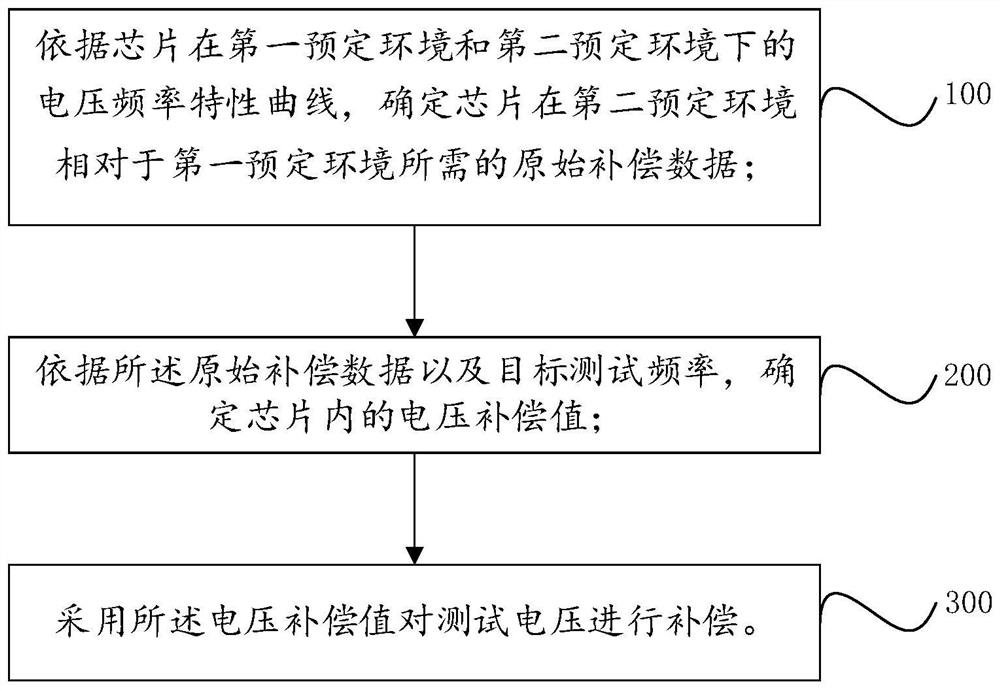
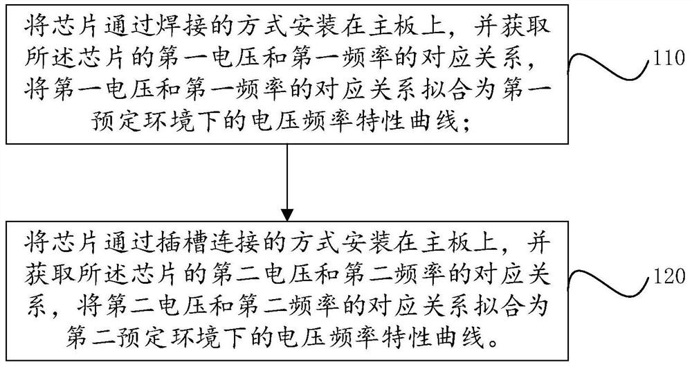
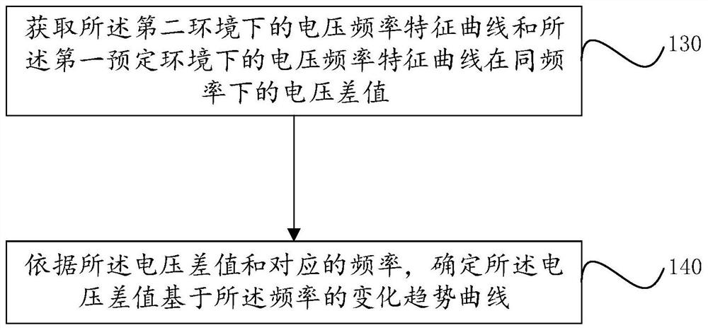
[0054] An embodiment of the present invention provides a chip system-level testing method, such as figure 1 shown, including:

[0055] Step 100, according to the voltage-frequency characteristic curves of the chip in the first predetermined environment and the second predetermined environment, determine the original compensation data require...


PUM


Abstract

The invention provides a chip system-level test method, which comprises the following steps of: determining original compensation data required by a chip in a second predetermined environment relative to a first predetermined environment according to voltage frequency characteristic curves of the chip in the first predetermined environment and the second predetermined environment; determining a voltage compensation value in the chip according to the original compensation data and a target test frequency; and compensating the test voltage by using the voltage compensation value. According to the chip system-level test method and device provided by the invention, the chip can work on the same voltage frequency curve characteristic curve in the test environment and the use environment, and the coverage range of the test is improved.

Description

technical field [0001] The invention relates to the technical field of chip testing, in particular to a chip system-level testing method and device. Background technique [0002] With the improvement of semiconductor design complexity and manufacturing process, ultra-high integration, ultra-high performance and ultra-high power consumption chips are becoming more and more mainstream, and the hardware design of chip application and testing is becoming more and more complex. Level Test (SLT for short) requirements and quality also bring huge challenges. [0003] At present, the system test SLT adopts a general-purpose hardware motherboard design, and generally uses a socket (referred to as socket) design to connect the chip and the motherboard. The test is performed according to the characteristic curve law of each chip and the voltage and frequency defined by the design specification. On the customer platform, a customized motherboard design is adopted according to actual ne...

Claims


Application Information

Patent Timeline
IPC IPC(8): G01R31/28
CPCG01R31/2851
Inventor 桂晓峰李育飞徐宏思刘署
Owner HYGON INFORMATION TECH CO LTD
Features
  • Generate Ideas
  • Intellectual Property
  • Life Sciences
  • Materials
  • Tech Scout
  • Unparalleled Data Quality
  • Higher Quality Content
  • 60% Fewer Hallucinations
Learn More