Tantalum carbide composite material

A composite material, tantalum carbide technology, applied in the direction of carbon compound, polycrystalline material growth, carbon preparation/purification, etc., can solve the problem of carbon material etching, etc., and achieve the effect of improving adsorption

Pending Publication Date: 2022-06-03
韩国东海炭素株式会社
View PDF5 Cites 0 Cited by
  • Summary
  • Abstract
  • Description
  • Claims
  • Application Information

AI Technical Summary

Problems solved by technology

[0004] According to these industrial needs, when directly using the carbon material used in the existing semiconductor process, there is a problem in susceptor parts commonly used i

Method used


Image

  • Tantalum carbide composite material
  • Tantalum carbide composite material
  • Tantalum carbide composite material

Examples


Example

[0057] Example 1 to Example 3

[0058] TaC was deposited on the graphite substrate using chemical vapor (CVD) deposition.

Example

[0059] Comparative Example 1 to Comparative Example 4

[0060] TaC was deposited on the graphite substrate using chemical vapor (CVD) deposition.

[0061] property analysis

[0062] (1) Analysis of surface microstructure

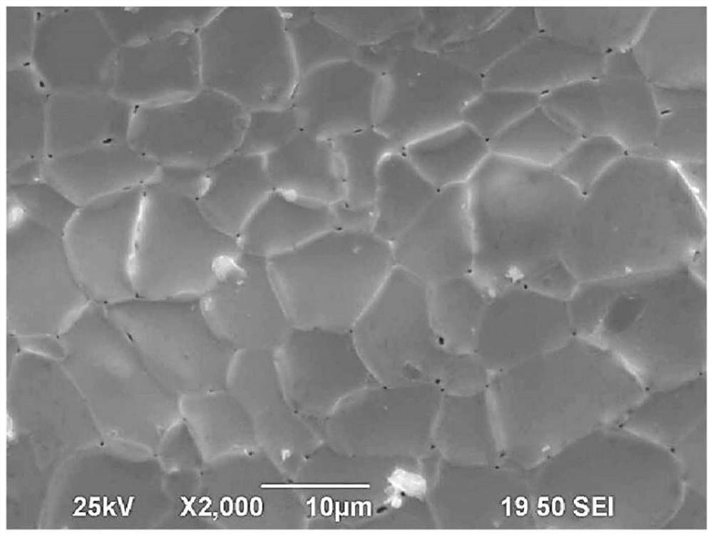
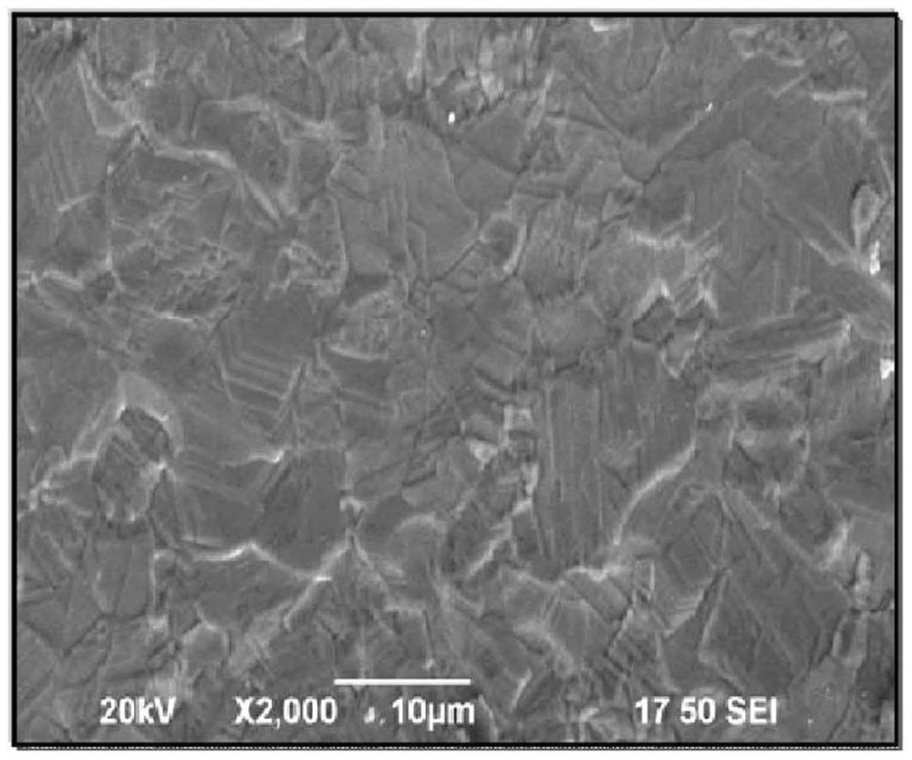
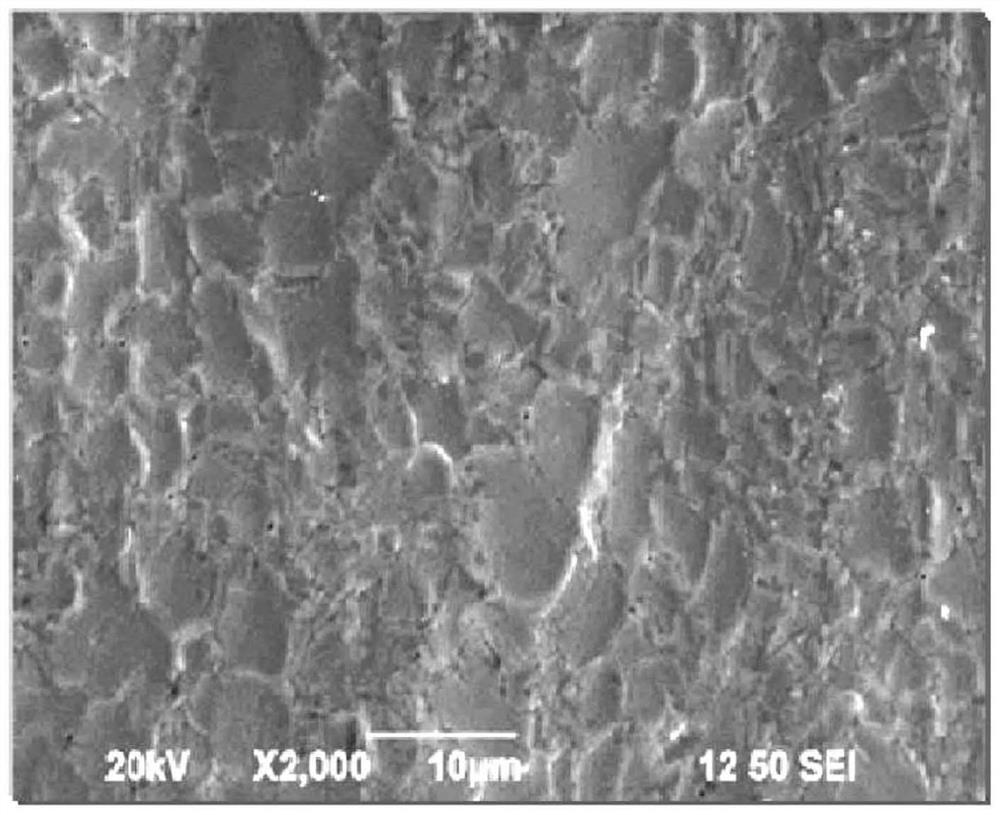
[0063] The surface microstructures of TaC prepared in Examples and Comparative Examples were observed by SEM, and the results are shown in Table 1 and Figure 1 to Figure 3 shown. In addition, in Table 1, the composition ratio of Ta and C is data measured by EDS, and is based on atomic (Atomic) % (model name: Oxford INCA x-act).

[0064] [Table 1]

[0065] Classification Comparative Example 1 Comparative Example 2 Example 1 Example 3 C(at%) 37.57 59.48 42.68 52.68 T(at%) 62.43 40.52 57.32 47.32 Ta / C 1.66 0.68 1.34 0.90 Surface shape of TaC particles wrinkled slightly wrinkled smooth smooth

[0066] Referring to Table 1, it can be seen that when the TaC surface microstructure is observed accor...


PUM


Abstract

The present invention relates to a tantalum carbide composite material, and more particularly, to a tantalum carbide composite material comprising a base material and a tantalum carbide film formed on the base material, the tantalum carbide film having a surface contact angle of 50 DEG or more and a low surface energy.

Description

technical field [0001] The invention relates to a tantalum carbide composite material. Background technique [0002] In recent years, there has been a need for a component material that minimizes processes such as precise process control and washing in semiconductor processing. That is, high-temperature growth equipment mainly used for SiC / AlN epitaxy (Epitaxy) or SiC / AlN growth (Growth) uses a radiation thermometer to measure the temperature, and uses the surface of the part as a radiation thermometer target (Target), however, there is a problem, That is, when process materials or particles, etc. are deposited on the target area, the temperature measurement becomes inaccurate. [0003] In addition, when process materials are easily deposited on the components, frequent cleaning of the components is required, and also affects the life of the components, which may further reduce the yield of the semiconductor device manufacturing process. Therefore, there is a need for a co...

Claims


Application Information

Patent Timeline
IPC IPC(8): C04B35/56C04B35/622C01B32/914
CPCC04B35/5607C04B35/62218C01B32/914C01P2002/72C01P2004/03C30B25/08C04B41/87C23C16/32C04B41/5057C04B41/009C04B35/522C04B41/4531C04B35/62222C01B32/05C01B32/21C30B29/36C30B29/40C30B23/02H01L21/67011C01P2002/70C01P2002/74C30B35/00
Inventor 曺东完
Owner 韩国东海炭素株式会社
Why Eureka
Try Eureka