Supercharge Your Innovation With Domain-Expert AI Agents!

Manufacturing method of semiconductor device

A manufacturing method and semiconductor technology, applied in the direction of semiconductor/solid-state device manufacturing, semiconductor devices, electrical components, etc., to achieve the effect of avoiding thickness reduction and height reduction

Inactive Publication Date: 2022-06-10
GUANGZHOU CANSEMI TECH INC
View PDF7 Cites 0 Cited by
  • Summary
  • Abstract
  • Description
  • Claims
  • Application Information

AI Technical Summary

Problems solved by technology

[0004] The object of the present invention is to provide a manufacturing method of a semiconductor device to solve the problem that the isotropic etching will reduce the height and thickness of the spacer layer at the same time

Method used


Image

  • Manufacturing method of semiconductor device
  • Manufacturing method of semiconductor device
  • Manufacturing method of semiconductor device

Examples


Embodiment Construction

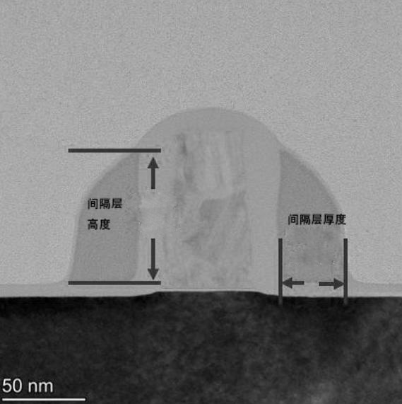
[0034] S6, performing ion implantation on the semiconductor substrate 1 using the remaining spacer layer 3 and the polysilicon 2 as a mask.

[0035] Wherein, as an example, the polysilicon 2 can be the gate of a MOS device. In step S6, using the spacer layer 3 and the polysilicon 2 as a mask, after ion implantation is performed on the semiconductor substrate 1 on both sides of the polysilicon, the polysilicon 2. A source region (not shown) and a drain region (not shown) of a MOS device are respectively formed in the semiconductor substrate 1 on both sides.

[0036] To sum up, in the manufacturing method of the semiconductor device provided by the embodiment of the present invention, by using the protective layer to protect the root of the spacer layer, on the basis of reducing the height of the spacer layer, it avoids the problems caused by conventional isotropic etching. Side effect of reduced spacer layer thickness.

[0037] The above description is only a description of th...


PUM


Abstract

The invention provides a manufacturing method of a semiconductor device, which comprises the following steps of: forming patterned polycrystalline silicon on a semiconductor substrate, and forming a spacer layer on the side wall of the polycrystalline silicon; covering a protective layer on the surface of the semiconductor substrate, wherein the protective layer exposes the tops of the polycrystalline silicon and the spacing layer and buries the spacing layer with a preset height inside; and etching to remove the exposed spacer layer, wherein the remaining spacer layer is the spacer layer required on the side wall of the polycrystalline silicon. After the spacer layer is normally etched and formed, the protective layer with a certain thickness is formed on the semiconductor substrate, the height of the spacer layer is reduced through etching, and the root part of the spacer layer is covered and protected by the protective layer, so that the side effect that the thickness of the spacer layer is reduced due to conventional isotropic etching is avoided in the isotropic etching process.

Description

technical field [0001] The invention relates to the technical field of semiconductor devices, in particular to a method for manufacturing a semiconductor device. Background technique [0002] The polysilicon spacer (POLY Spacer, also known as the polysilicon sidewall) is used to protect the polysilicon (POLY) sidewall and define the area for subsequent ion implantation (IMP). Among them, spacer height and spacer width are two very important parameters. like figure 1 As shown, the height of the spacer layer is used to characterize the protection area of ​​the spacer layer for the polysilicon sidewall. If the spacer layer is too high or too low, it will have a direct impact on the protection area of ​​the polysilicon itself, and will also affect the subsequent nickel silicide (Nickle Silicide, referred to as NiSi) and other metal silicide formation conditions. The thickness of the spacer layer is more used to define the region for subsequent ion implantation. [0003] In t...

Claims


Application Information

Patent Timeline
Patent Type & Authority Applications(China)
IPC IPC(8): H01L21/311H01L21/336H01L21/28
CPCH01L21/31138H01L21/31116H01L21/28008H01L29/6653
Inventor 廖军洪明杰
Owner GUANGZHOU CANSEMI TECH INC
Features
  • R&D
  • Intellectual Property
  • Life Sciences
  • Materials
  • Tech Scout
  • Unparalleled Data Quality
  • Higher Quality Content
  • 60% Fewer Hallucinations
Learn More