
Inverted-structure perovskite QLED device based on photoetching technology and preparation method thereof

An inverted structure and photolithography technology, which is applied in semiconductor/solid-state device manufacturing, semiconductor devices, electric solid-state devices, etc., can solve problems such as instability, incompatible surface ligands, and affecting the application of perovskite QLED devices, and achieve Achieving a patterned effect

Pending Publication Date: 2022-06-21
FUZHOU UNIV
View PDF0 Cites 0 Cited by
  • Summary
  • Abstract
  • Description
  • Claims
  • Application Information

AI Technical Summary

Problems solved by technology

However, due to the incompatibility of perovskite materials with polar solvents and the instability of surface ligands, it is a huge challenge to realize the patterning of perovskite quantum dots, which affects the application of perovskite QLED devices.

Method used


Image

  • Inverted-structure perovskite QLED device based on photoetching technology and preparation method thereof
  • Inverted-structure perovskite QLED device based on photoetching technology and preparation method thereof

Examples


preparation example Construction

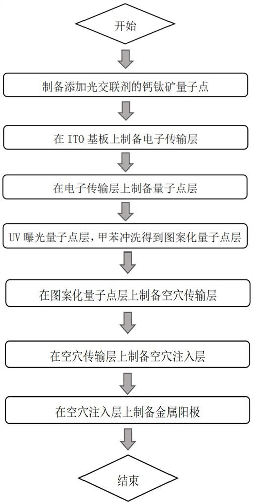
[0021] 2) Put the cathode substrate into glass cleaning agent, deionized water, acetone, and ethanol in sequence for ultrasonic treatment, and the time for each ultrasonic is 10 minutes.

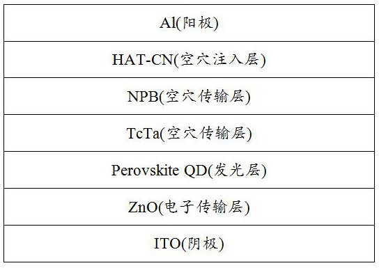
[0022] 3) ZnO was prepared as an electron transport layer by spin-coating method with an annealing temperature of 150 °C and a thickness of about 50 nm.

[0023] 4) Spin-coat perovskite quantum dots added with a photocrosslinking agent on the surface of the electron transport layer by spin coating as a patterned quantum dot layer, with a thickness of about 30 nm. The quantum dot ligands in the exposed part are crosslinked under UV light through a photolithography process, rinsed with toluene after exposure, and what remains is the patterned quantum dot layer after the crosslinking of the quantum dot ligands.

[0024] 5) Evaporate TcTa as a hole transport layer by vacuum evaporation method, and its thickness is 30 nm.

[0025] 6) Evaporate NPB as a hole transport layer by vacuum evaporation ...

Embodiment 1


PUM

PropertyMeasurementUnit
Thicknessaaaaaaaaaa
Thicknessaaaaaaaaaa

Abstract

The invention relates to an inverted-structure perovskite QLED device based on a photoetching process. The inverted-structure perovskite QLED device comprises a transparent conductive substrate ITO, and an electron transport layer, a patterned quantum dot film, a hole transport layer, a hole injection layer and a metal anode which are sequentially deposited on the transparent conductive substrate ITO layer. According to the method, the defect that the perovskite quantum dots are incompatible with a traditional photoetching process is overcome, the influence of the solvent on the functional layer is also overcome, and patterning of the perovskite quantum dots and preparation of a QLED device can be achieved.

Description

technical field [0001] The invention belongs to the field of display technology, and relates to an inverted structure perovskite QLED device based on a photolithography process and a preparation method thereof. Background technique [0002] Lead halide perovskite quantum dots have been proven to be excellent materials for quantum dot light-emitting diodes (QLEDs), photodetectors, solar cells, and lasers due to their advantages such as tunable wavelength, high optical absorption coefficient, and narrow half-peak width. Various methods for patterning perovskite materials have been developed, including photolithography, micro / nanoimprinting, inkjet printing, X-ray lithography, electron beam lithography, etc. Among these technologies, photolithography is the most promising patterning method because of its mature process and easy implementation of colored pixel arrays. Photoresists in traditional photolithography processes cannot be used in electroluminescent devices because the...

Claims


Application Information

Patent Timeline
IPC IPC(8): H01L51/50H01L51/56
CPCH10K71/12H10K50/115
Inventor 胡海龙郄媛李福山郭太良鞠松蔓
Owner FUZHOU UNIV
Features
  • Generate Ideas
  • Intellectual Property
  • Life Sciences
  • Materials
  • Tech Scout
  • Unparalleled Data Quality
  • Higher Quality Content
  • 60% Fewer Hallucinations
Learn More