Supercharge Your Innovation With Domain-Expert AI Agents!

Image sensor, image sensor test system and method

An image sensor and test system technology, applied in image communication, TV system components, instruments, etc., can solve problems such as image signal distortion and image impact

Pending Publication Date: 2022-07-19
SK HYNIX INC
View PDF0 Cites 0 Cited by
  • Summary
  • Abstract
  • Description
  • Claims
  • Application Information

AI Technical Summary

Problems solved by technology

[0004] Electrical signals generated by an array of pixels in an image sensor may include noise that may adversely affect the quality of the image
[0005] Examples of noise include dark current, a relatively small current that flows through a photosensitive device such as a photodiode even if no photons enter the device, which results in distortion of the image signal

Method used


Image

  • Image sensor, image sensor test system and method
  • Image sensor, image sensor test system and method
  • Image sensor, image sensor test system and method

Examples


Embodiment Construction

[0018] Features of the technology disclosed in this patent document are described by way of example of an image sensing device with reference to the accompanying drawings.

[0019] Although some implementations of the disclosed technology will be discussed, the disclosed technology can be implemented in various ways beyond the details of the examples described herein.

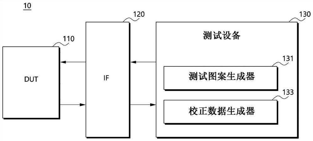
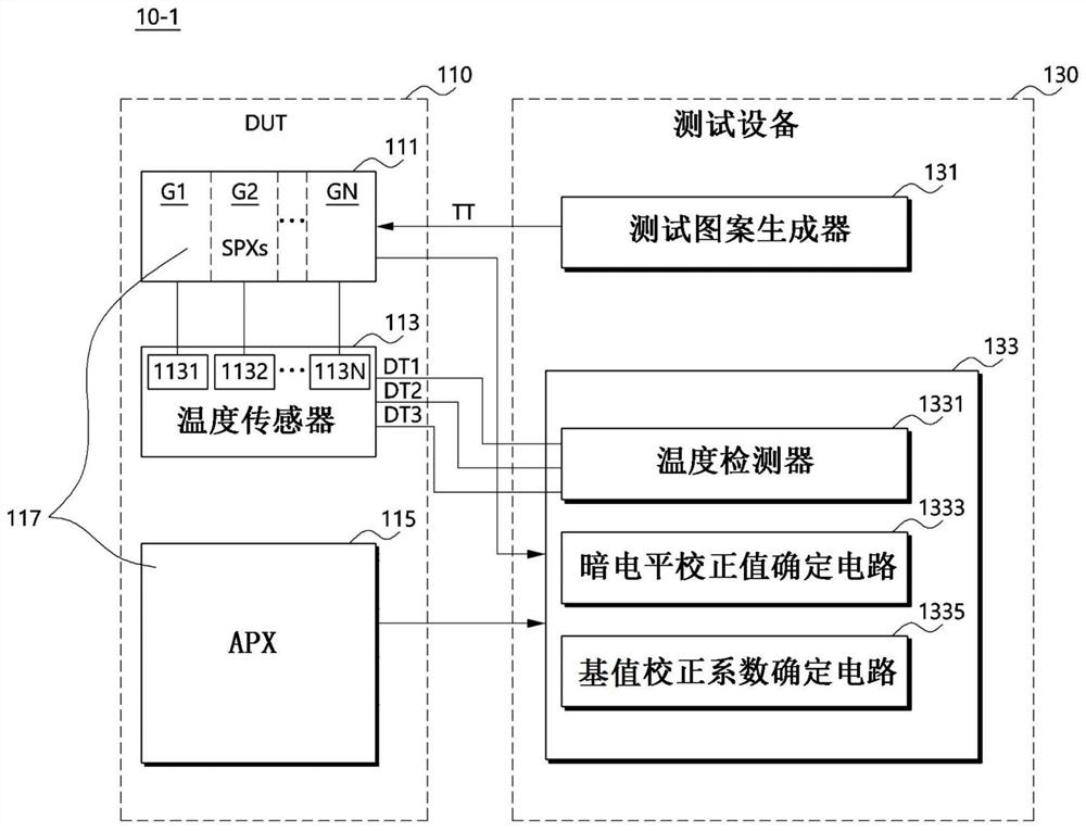
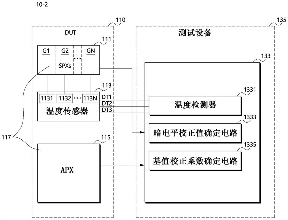
[0020] figure 1 An image sensor test system based on an example implementation of the disclosed technology is shown.

[0021] refer to figure 1 , the image sensor test system 10 may include a device under test (DUT) 110, a test equipment 130 coupled to the DUT 110 to perform tests on the DUT 110, and a test device 130 coupled between the DUT 110 and the test equipment 130 as a function of the DUT 110 and the test equipment 130 An interface circuit (IF) 120 that transmits signals between the electrical interfaces.

[0022] DUT 110 may include at least one image sensor to be tested. In some implementations, D...


PUM


Abstract

The invention relates to an image sensor, an image sensor testing system and an image sensor testing method. An image sensor may include: an active pixel array including a plurality of active pixels operable to convert incident light into pixel signals of image information carried in the incident light; a plurality of sampling pixel groups located adjacent to the active pixel array but spatially separated from the active pixel array, and having different heat dissipation characteristics from the other sampling pixel groups; and a plurality of temperature sensors respectively coupled to the sampling pixel groups to provide temperature measurements.

Description

technical field [0001] The techniques and implementations disclosed in this patent document relate generally to a semiconductor integrated device, and more particularly, to an image sensor and an image sensor testing system and method. Background technique [0002] The image sensor includes a pixel array including optoelectronic semiconductor devices and transistors. Optoelectronic semiconductor devices can convert light into photoelectric charges. Transistors can convert photocharges generated by optoelectronic semiconductor devices into electrical signals. [0003] A CMOS image sensor may include a single integrated circuit (IC) in which an analog control circuit and a digital control circuit are integrated. CMOS image sensors can convert light reflected from objects and incident on opto-semiconductor devices of a pixel array into electrical charges. The amount of accumulated charge is proportional to the voltage signal generated by the CMOS image sensor. [0004] The ...

Claims


Application Information

Patent Timeline
Patent Type & Authority Applications(China)
IPC IPC(8): H04N5/361H04N5/217H04N5/378H04N5/3745H04N17/00G01K7/01
CPCH04N17/00G01K7/01H04N25/77H04N25/633G01K1/026G01K13/00H04N17/002H01L27/14621H01L27/14627H04N25/11H04N25/63
Inventor 李殷光
Owner SK HYNIX INC
Features
  • R&D
  • Intellectual Property
  • Life Sciences
  • Materials
  • Tech Scout
  • Unparalleled Data Quality
  • Higher Quality Content
  • 60% Fewer Hallucinations
Learn More