Supercharge Your Innovation With Domain-Expert AI Agents!

Semiconductor process equipment and processing method thereof

A processing method and technology of process equipment, applied in semiconductor/solid-state device manufacturing, cleaning methods and utensils, chemical instruments and methods, etc., can solve the problems of wafer contamination, affecting the process yield of semiconductor process equipment, etc. The effect of reducing application and maintenance costs and improving economic efficiency

Pending Publication Date: 2022-08-05
BEIJING NAURA MICROELECTRONICS EQUIP CO LTD
View PDF0 Cites 0 Cited by
  • Summary
  • Abstract
  • Description
  • Claims
  • Application Information

AI Technical Summary

Problems solved by technology

[0004] In view of the shortcomings of the existing methods, this application proposes a semiconductor process equipment and its processing method to solve the technical problem in the prior art that the wafer is polluted due to the peeling off of the oxide film, thereby affecting the process yield of the semiconductor process equipment

Method used


Image

  • Semiconductor process equipment and processing method thereof
  • Semiconductor process equipment and processing method thereof
  • Semiconductor process equipment and processing method thereof

Examples


Embodiment Construction

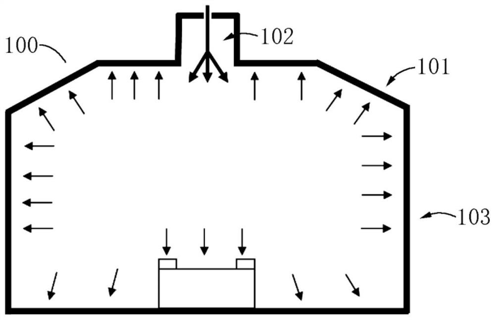
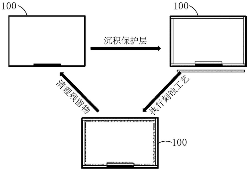
[0026] The application is described in detail below, and examples of embodiments of the application are illustrated in the accompanying drawings, wherein the same or similar reference numerals refer to the same or similar components or components having the same or similar functions throughout. Also, detailed descriptions of known technologies are omitted if they are not necessary for illustrating features of the present application. The embodiments described below with reference to the accompanying drawings are exemplary and are only used to explain the present application, but not to be construed as a limitation on the present application.

[0027] It will be understood by those skilled in the art that, unless otherwise defined, all terms (including technical and scientific terms) used herein have the same meaning as commonly understood by one of ordinary skill in the art to which this application belongs. It should also be understood that terms, such as those defined in a g...


PUM


Abstract

The embodiment of the invention provides semiconductor process equipment and a processing method thereof. The processing method of the semiconductor process equipment is used for processing the interior of a process chamber before a wafer is subjected to a process, and comprises the following steps: cleaning residues in the process chamber; depositing a first compact oxide layer on the inner wall of the cleaned process chamber; and densifying the first dense oxide layer to form a second dense oxide layer on the surface of the first dense oxide layer, the oxygen content of the second dense oxide layer being greater than the oxygen content of the first dense oxide layer. According to the embodiment of the invention, the first compact oxide layer and the second compact oxide layer are formed on the inner wall of the process chamber, and the compactness of the second compact oxide layer is better, so that the second compact oxide layer does not peel off into particles due to looseness in the etching process, the wafer is prevented from being polluted, and the yield of the etching process is greatly improved.

Description

technical field [0001] The present application relates to the technical field of semiconductor processing, and in particular, the present application relates to a semiconductor processing equipment and a processing method thereof. Background technique [0002] At present, with the rapid development of the information age, the semiconductor manufacturing industry is also developing rapidly. With the in-depth research in the technical field, the entire manufacturing industry is paying more and more attention to cost saving. For the etching equipment of semiconductor process equipment, the loss of parts exposed to the plasma etching surface inside the process chamber is particularly serious, and with the loss of parts inside the process chamber, the etching environment in the process chamber will drift, so This will further lead to instability of some key dimensions of the etching process. In order to make the etching environment of the process chamber consistent, the internal ...

Claims


Application Information

Patent Timeline
Patent Type & Authority Applications(China)
IPC IPC(8): H01L21/67B08B13/00
CPCH01L21/67207B08B13/00
Inventor 汤中海张建坤赵尊华胡海洋桑强强蔡亲华
Owner BEIJING NAURA MICROELECTRONICS EQUIP CO LTD
Features
  • R&D
  • Intellectual Property
  • Life Sciences
  • Materials
  • Tech Scout
  • Unparalleled Data Quality
  • Higher Quality Content
  • 60% Fewer Hallucinations
Learn More