Word line driver of semiconductor memory device
A word line driver, storage device technology, applied in static memory, digital memory information, information storage, etc., can solve problems such as large space, loss of chip area, and difficulty in implementing negative voltage converters
- Summary
- Abstract
- Description
- Claims
- Application Information
AI Technical Summary
Problems solved by technology
Method used
Image

Examples
Embodiment 1
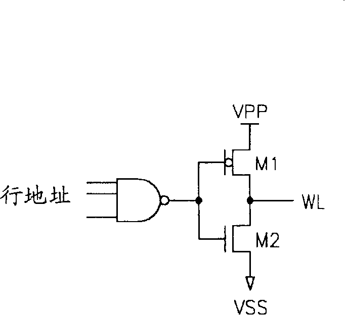
[0033] attached Figure 4 Shown is a first embodiment of a memory device according to the invention. in the attached Figure 4 The drive circuit shown in is configured so that it keeps the word line WL at Vbb after the precharge operation, but diverts most of the word line discharge current to Vss, thereby reducing the need for a negative supply. attached Figure 4 The driver circuit of the present invention includes a power hold circuit (or “hold circuit”) 20 and a driver stage 18 with a modified driver section 22 . The hold circuit 20 includes an NMOS transistor M4 having a channel connected between WL and Vbb and a gate connected to the output of an inverter INV1 and a substrate connected to Vbb. Inverter INV1 is referenced to Vbb and has an input connected to a word line. In the modified driver section 22, a diode connecting the NMOS transistor M3 is connected in series with M2. The substrates of both M2 and M3 are connected to Vbb. The holding circuit 20 is preferab...
Embodiment 2
[0039] attached Figure 5 Shown is a second embodiment of a memory device according to the invention. in the attached Figure 5 The drive circuit shown in the attached Figure 4 The drive circuit differs in the attached Figure 5 No hold circuit is required in , and a further modification is made to the modified driver section 24, including a larger NMOS pull-down transistor M2. The source of M2 is connected to Vbb and the gate of M3 is connected together with the gate of M2 to the output of the row decoder. The channel of M4 is connected between the drain of M2 and Vss, and the gate of M4 is connected to the word line WL. The substrates of M2, M3 and M4 are all connected to Vbb. Thus, transistor M4 diverts the wordline discharge current to Vss by coupling the wordline to Vss in response to the wordline voltage whenever M3 is now on. Transistor M2 now couples the word line to Vbb in response to the row address information.
[0040] At the end of the access operation, th...
Embodiment 3
[0043] attached Figure 6 Shown is a third embodiment of a memory device according to the invention. in the attached Figure 6 The structure and operation of the drive circuit shown in the attached Figure 5 The structure and operation of the drive circuit is similar, but the transistor M3 has been changed to be in series with M4 instead of M2.
[0044] Sub word line drive scheme
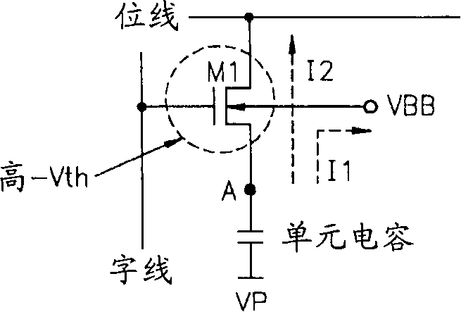
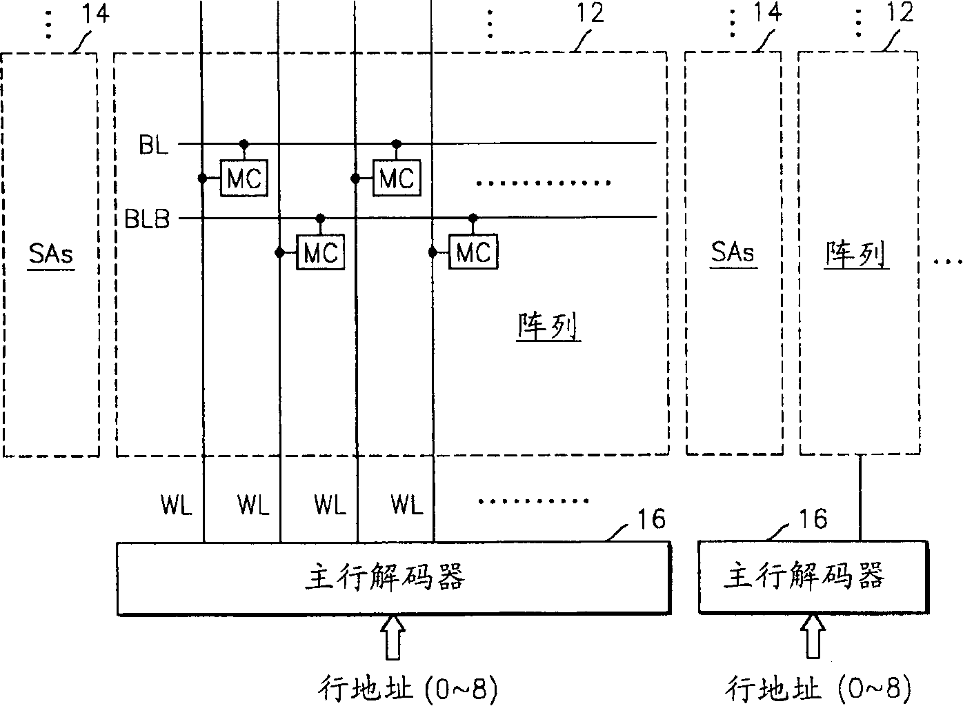
[0045] The principles of the present invention discussed above with respect to memory devices having a main wordline scheme can be extended to other types of memory devices including, for example, memory devices utilizing sub-wordline driving schemes. attached Figure 7 Shown is the core structure of a typical prior art DRAM device utilizing a sub-word line driving scheme. Although memory devices of this type are disclosed in US Pat. Nos. 5,416,748, 5,596,542, 5,764,585, 5,781,498, and 5,986,966, memory devices of this type are briefly summarized here for convenience...
PUM
 Abstract
Description
Claims
Application Information
 - R&D Engineer
- R&D Manager
- IP Professional
- Industry Leading Data Capabilities
- Powerful AI technology
- Patent DNA Extraction
Browse by: Latest US Patents, China's latest patents, Technical Efficacy Thesaurus, Application Domain, Technology Topic.
© 2024 PatSnap. All rights reserved.Legal|Privacy policy|Modern Slavery Act Transparency Statement|Sitemap