Check patentability & draft patents in minutes with Patsnap Eureka AI!

Power source circuit device

A power circuit, high potential technology, applied in the direction of circuits, electrical components, electric solid devices, etc., can solve the problems that the pin structure cannot fully ensure the distance along the surface, the product operation is not safe, and cannot meet safety standards, etc.

Inactive Publication Date: 2003-12-17
SEMICON COMPONENTS IND LLC
View PDF0 Cites 8 Cited by
  • Summary
  • Abstract
  • Description
  • Claims
  • Application Information

AI Technical Summary

Problems solved by technology

In the existing structure, even if the pins are bent up and down, the safety standard may not be met when the distance along the surface can only be guaranteed to be 1.7 mm.
That is, the existing pin structure cannot sufficiently ensure the distance along the surface
[0007] Moreover, although the top 14h part of the existing package that is integrated with the third pin is connected to a high-potential drain such as 800 volts, it is also made into an exposed structure, which is not safe in terms of product operation. The problem

Method used


Image

  • Power source circuit device
  • Power source circuit device
  • Power source circuit device

Examples


Embodiment Construction

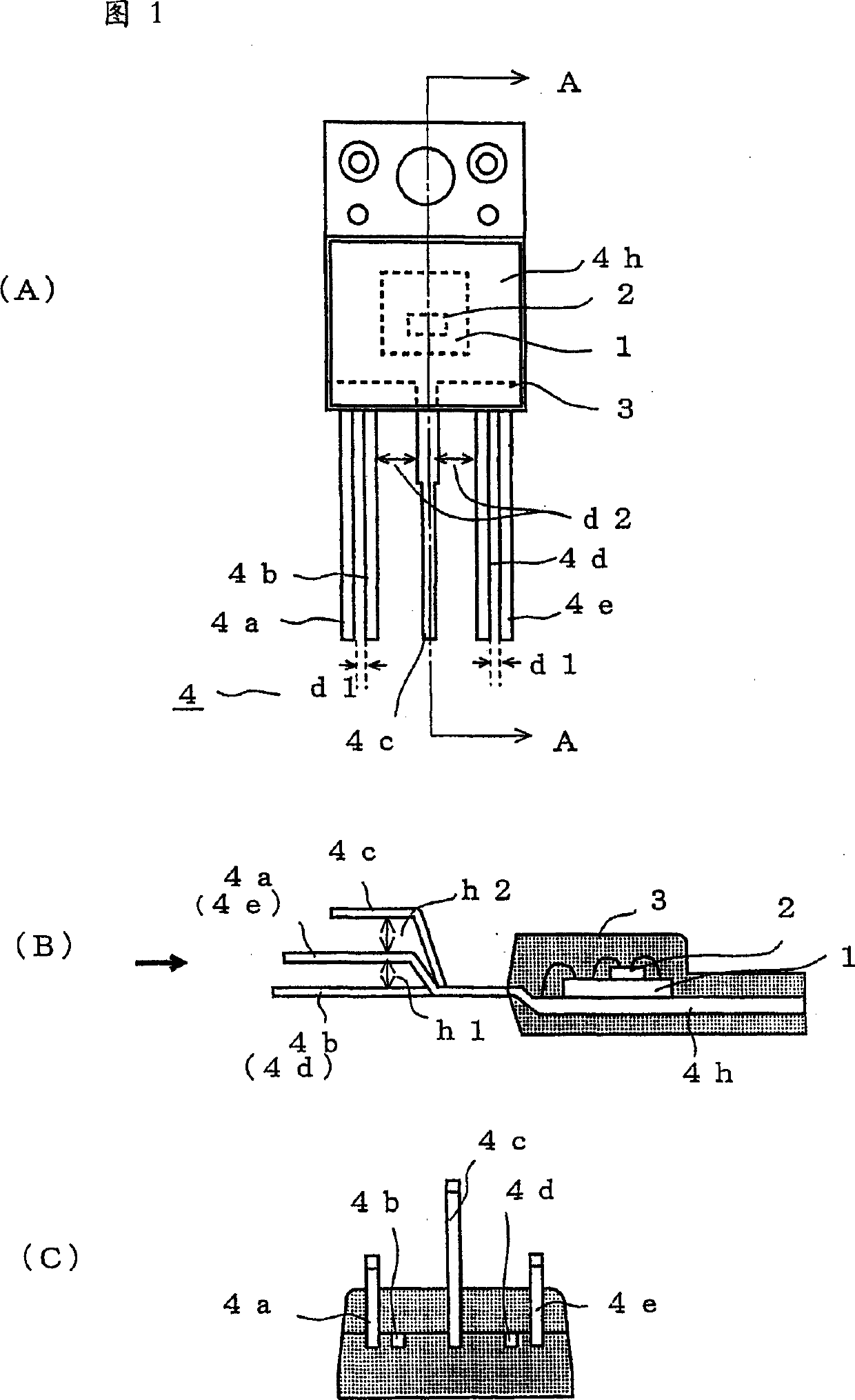
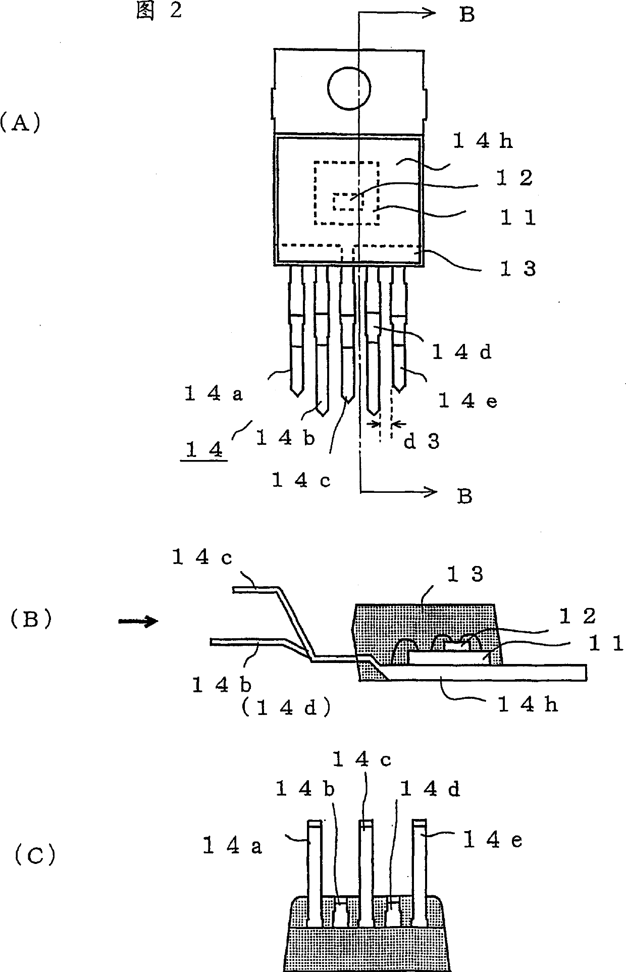
[0023] Taking a package with 5 pins as an example, a specific embodiment of the present invention will be described in detail with reference to FIG. 1 .

[0024] Fig. 1 (A) is a top view, Fig. 1 (B) is the A-A sectional view of Fig. 1 (A), and Fig. 1 (C) is a side view of Fig. 1 (B) seen from the arrow direction.

[0025] The power supply circuit device of the present invention is composed of MOSFET1, IC2, package 3 and five pins 4.

[0026] The MOSFET 1 includes a plurality of MOSFET elements, the inside of which is a drain electrode, and is fixed to the top 4h integrally connected with the third pin 4c with a conductive adhesive (see FIG. 1(B)).

[0027] IC2 is mounted on MOSFET1 and connected to the power electrode and drain electrode of MOSFET1. And each control terminal is connected to the 1st pin 4a, the 2nd pin 4b, and the 4th pin 4d (refer FIG.1(B)).

[0028] Package 3 seals MOSFET1 and IC2 with insulating resin by transfer molding or the like. Since the package 3 i...


PUM


Abstract

In a conventional power circuit device, such as a power MOSFET monolithic integrated circuit device and a compound device, since five lead pins are lead out from the packaging with even intervals, sufficient separation distances between the third pin of a high voltage and other adjacent pins cannot be secured. According to this invention, the distances between the third pin and other adjacent pins are expanded so as to become wider than the distances between other pins. Furthermore, the third pin is formed into an upper position, its adjacent pins are formed into a lower position, and other pins are formed into a middle position. Thereby, sufficient separation distances between the third pin of the high voltage and other adjacent pins can be secured. Therefore, a structure favorable in terms of safety can be provided. Furthermore, by providing a full-mold packaging, the header portion is not exposed to assure an easy handling.

Description

technical field [0001] The present invention relates to a power circuit device, and more particularly to a power circuit device using an IC package in which lead wires introduced from a package body have been improved in shape. Background technique [0002] As is well known, an IC package in which an IC chip and lead wires (leads) are connected by wire bonding or the like, and a package main body made of resin serves as an exterior package is used. [0003] Fig. 2 shows the situation that there are 5 pins to the existing IC package, Fig. 2 (A) is a top view, Fig. 2 (B) is a B-B sectional view of Fig. 2 (A), Fig. 2 (C) is from the direction of the arrow Look at the side view of Figure 2(B). [0004] For monolithic integrated circuits and composite components including power MOSFET11, in order to mount IC12 on power MOSFET11, five pins with equal spacing (d3) are generally used. According to FIG. 2(A), five pins 14 are arranged on one side wall of the package body 13 . At t...

Claims


Application Information

Patent Timeline
Patent Type & Authority Applications(China)
IPC IPC(8): H01L23/495
CPCH01L2924/13091H01L23/49562H01L2224/32145H01L23/49575H01L2924/01004H01L24/48H01L2224/48145H01L2224/48091H01L2224/48247H01L2924/14H01L2924/181H01L2924/00014H01L2924/00H01L2924/00012H01L2224/45099H01L2224/45015H01L2924/207H01L23/48
Inventor 土田满穗池田宪史西川円
Owner SEMICON COMPONENTS IND LLC
Features
  • R&D
  • Intellectual Property
  • Life Sciences
  • Materials
  • Tech Scout
  • Unparalleled Data Quality
  • Higher Quality Content
  • 60% Fewer Hallucinations
Learn More