Supercharge Your Innovation With Domain-Expert AI Agents!

Event-driven logic circuit

A logic circuit and event technology, applied in the field of logic circuits, can solve problems such as increased input load, increased activation rate of dynamic circuits, and high activation rate

Inactive Publication Date: 2006-02-08
PANASONIC CORP
View PDF2 Cites 0 Cited by
  • Summary
  • Abstract
  • Description
  • Claims
  • Application Information

AI Technical Summary

Problems solved by technology

[0005] However, the following problem has been pointed out: in the dynamic circuit, since the initialization phase and the evaluation phase are alternately operated continuously, the activation rate is higher than that of the static circuit
Due to the principle of detecting changes in input signals, the application of clock control corresponding to changes in input signals is limited to sequential elements such as flip-flops and memories.
[0010] In this way, the increase of the input load in the static circuit, the increase of the activation rate in the dynamic circuit and the difficulty of the design, the occurrence of the overhead of the handshake circuit in the asynchronous circuit and the difficulty of the design, and the difficulty of the design according to the input signal Applicable restrictions in changing clock control, etc., make it difficult for logic circuits to achieve high speed and low power consumption at the same time
As in static circuits, the results of evaluating signals input to functions are propagated successively, or as in dynamic circuits, the results of evaluating signals are input to functions at intervals are propagated. As long as the circuit operation is based on one of these methods, it is difficult to solve it at the same time. Issues such as signal loading, activation rate, and circuit size

Method used


Image

  • Event-driven logic circuit
  • Event-driven logic circuit
  • Event-driven logic circuit

Examples


no. 1 example

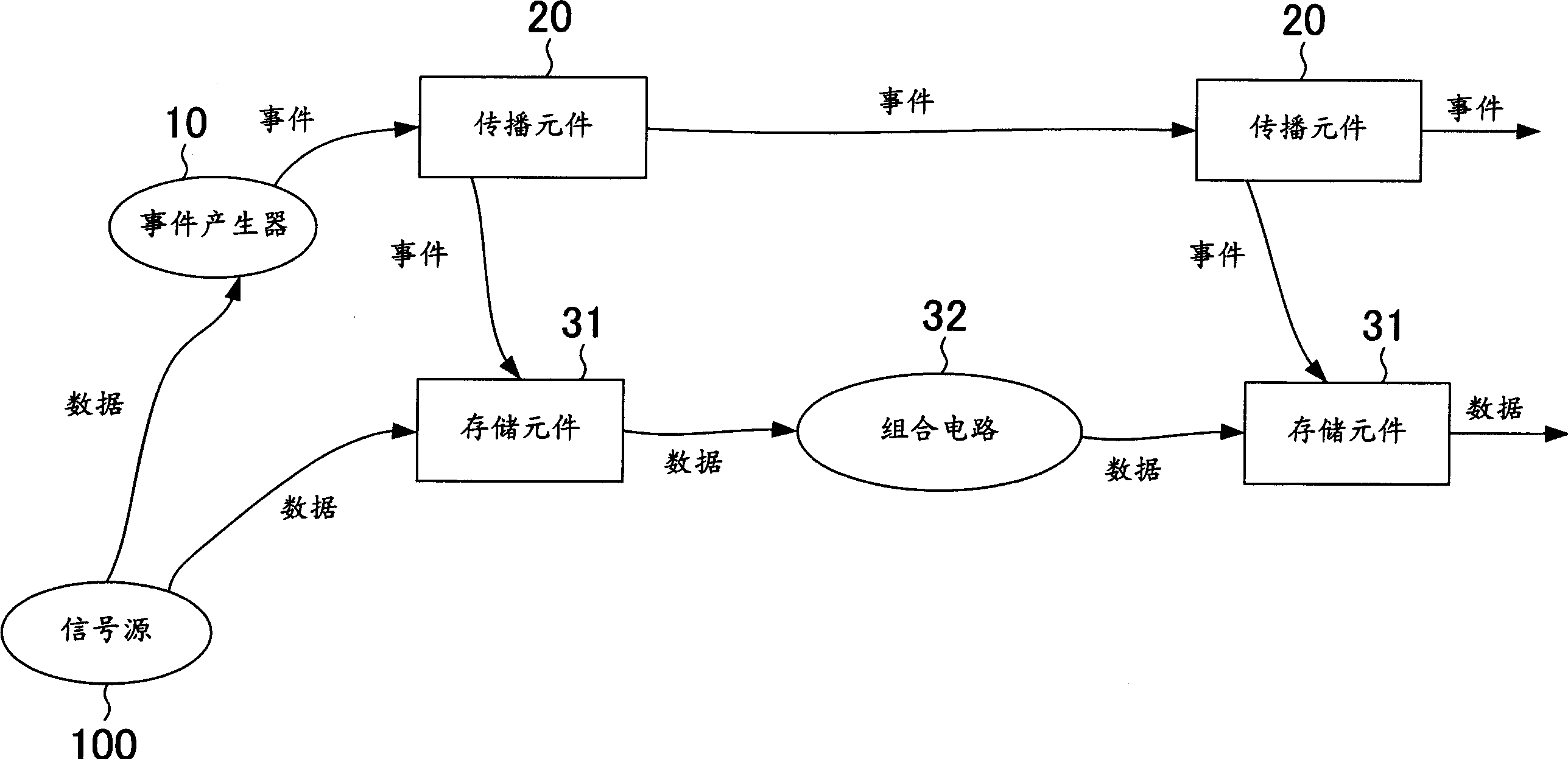
[0084] image 3 This is the schematic configuration of the logic circuit according to the first embodiment of the present invention. The logic circuit according to this embodiment includes a storage element 31 storing input data as an evaluation element. The operation of the logic circuit involved in this embodiment is as follows: First, as the output of the signal source 100 changes, the event generated in the event generator 10 is propagated in each propagation element 20 . The first-stage storage element 31 stores data output from the signal source 100 according to an event sent from the first-stage propagation element 20 . The data stored in the storage element 31 of the first stage is subjected to a logical operation by the combinational circuit 32, and the operation result is provided to the storage element 31 of the next stage. The next-level storage element 31 stores the data received from the combinational circuit 32 according to the event sent by the corresponding ...

no. 2 example

[0087] Figure 4 The circuit configuration of the evaluation element according to the second embodiment of the present invention is shown. The evaluation element according to this embodiment includes a capacitor 301, a charge and discharge controller 302 that controls charging and discharging of electric charges to and from the capacitor 301 according to events, a charging element 303 that charges the capacitor 301 under the control of the charge and discharge controller 302, and The discharge element 304 to be discharged determines the function-based discharge path evaluation logic circuit 305 and a static gate 306 such as an inverter. In addition, the capacitor 301 is preferably made of ferroelectric.

[0088] Next, refer to Figure 5 The timing chart of , illustrates the operation of the evaluation element involved in this embodiment. First, the charging element 303 operates by the generation of an event, and the charge holding state of the capacitor 301 is initialized. ...

no. 3 example

[0091] Image 6 A schematic configuration of a logic circuit according to a third embodiment of the present invention is shown. In the logic circuit according to the present embodiment, the evaluation element 30 includes an evaluation controller 40 that receives events from the propagation element 20 and outputs various control signals and substrate bias voltages, and inputs an input based on the control performed by the evaluation controller 40 . The evaluation unit 30' that evaluates the obtained data.

[0092] Figure 7 The circuit configuration of the evaluation element according to this example is shown. In addition, description of the evaluation controller is omitted. The evaluation element involved in this embodiment includes: an element 303 that controls the precharge operation according to the provided initialization control signal, an element 304 that controls the evaluation operation according to the provided evaluation control signal, and an evaluation logic cir...


PUM


Abstract

A logic circuit comprises: an event generator (10) for detecting a variation in data outputted from a signal source (100) to generate an event which indicates the variation of the data; a plurality of propagation elements (20) for propagating the event in a chained fashion; and a plurality of evaluation elements (30) for evaluating data received at a first stage from the signal source (100) to propagate a result of the evaluation in a chained fashion. When receiving the event, each of the plurality of evaluation elements (30) evaluates the data inputted to the evaluation element. A logic circuit is realized wherein both an input load and an activation yield are reduced, and a high speed operation is realized with low power consumption.

Description

technical field [0001] The present invention relates to a logic circuit, in particular to a circuit structure technique for reducing delay and power consumption of sequential circuits. Background technique [0002] In current semiconductor integrated circuits, static circuits centered on CMOS (Complementary Metal Oxide Semiconductor) circuits are widely used. CMOS circuits have the following advantages: If the input does not change, the output does not change, and the current consumption is only a small leakage component and the activation component generated when the value shifts, and the current consumption is small. The disadvantages of the CMOS circuit can be cited as follows: the power delay product is relatively large when realizing high-speed operation. [0003] Figure 62 It is a diagram showing a CMOS circuit based on a concept. In general, a CMOS circuit has a circuit for realizing a logic operation of an evaluation function f and a complementary function f* whic...

Claims


Application Information

Patent Timeline
IPC IPC(8): H03K19/017H03K19/0948
Inventor 笹川幸宏高畑敦志
Owner PANASONIC CORP
Features
  • R&D
  • Intellectual Property
  • Life Sciences
  • Materials
  • Tech Scout
  • Unparalleled Data Quality
  • Higher Quality Content
  • 60% Fewer Hallucinations
Learn More