Check patentability & draft patents in minutes with Patsnap Eureka AI!

Automatic testing system for light transient

An automatic test system, transient technology, applied in optical testing flaws/defects, single semiconductor device testing, measuring devices, etc., can solve the problems of complicated data processing, difficult to determine the peak value of equipment spectrum, etc.

Inactive Publication Date: 2006-06-14
INST OF SEMICONDUCTORS - CHINESE ACAD OF SCI
View PDF0 Cites 4 Cited by
  • Summary
  • Abstract
  • Description
  • Claims
  • Application Information

AI Technical Summary

Problems solved by technology

It can solve the problem that the peak value of the original equipment spectrum is difficult to determine and the data processing is cumbersome

Method used


Image

  • Automatic testing system for light transient

Examples


Embodiment Construction

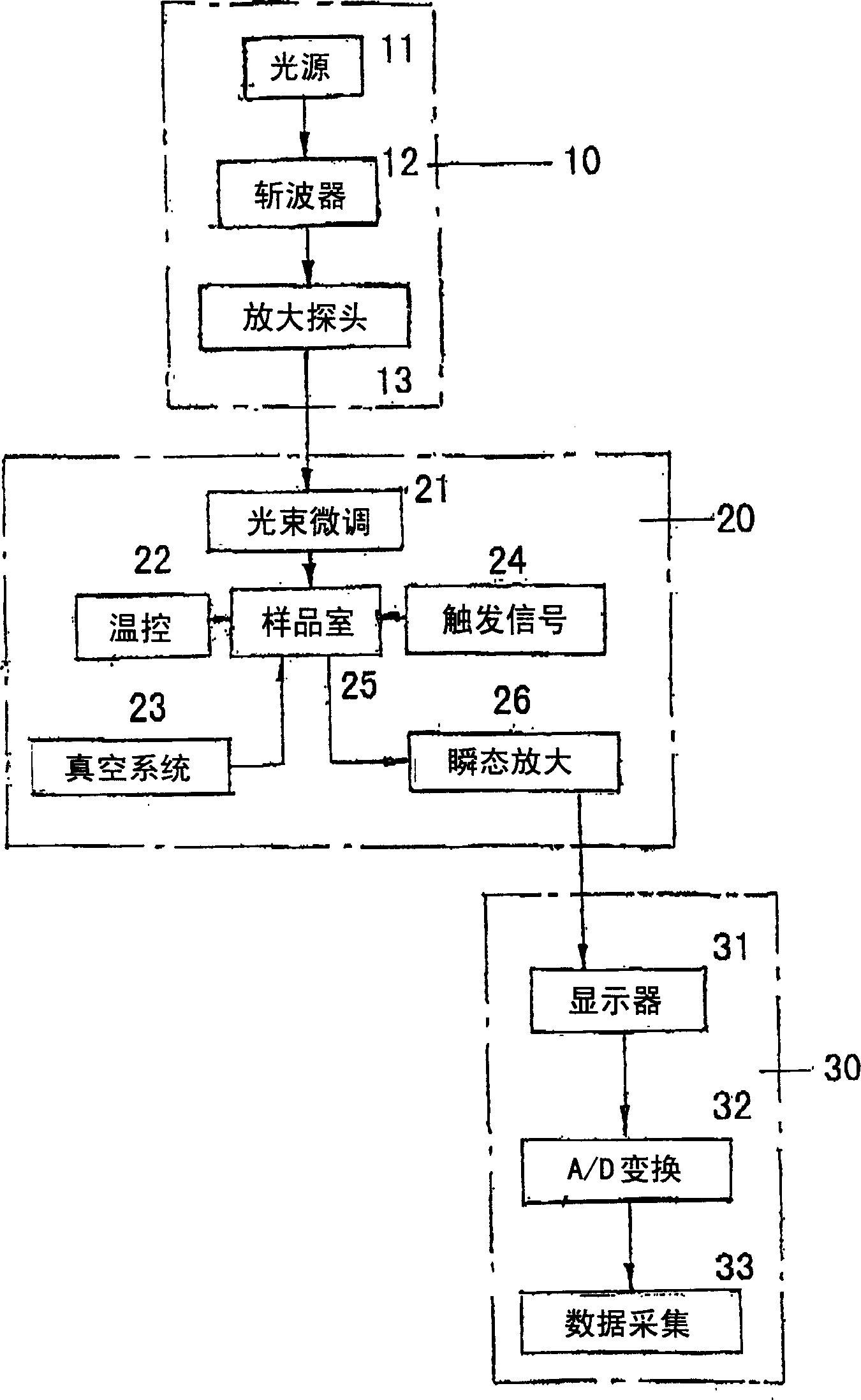
[0031] Attached below Figure 1 A further detailed description is made on the optically excited transient automatic test system.

[0032] figure 1 Among them, it is divided into three parts:

[0033] The first part is a diagram of the light injection device of the present invention.

[0034] The second part is the diagram of the sample chamber device of the present invention.

[0035] The third part is a diagram of the information collection and processing device of the present invention.

[0036] figure 1 Among them, the light injection device 10; is fixed on a movable track by the white light source 11, after the light passes through the chopper 12 fixed on the same track, the required wavelength can be obtained, and then through the amplifying probe 13, and The quartz optical fiber is transmitted to the micro-motion frame fixed on the light port of the upper cover of the sample chamber.

[0037] Sample chamber device 20: a three-dimensional micro-motion adjustment fra...


PUM


Abstract

The invention relates to semiconductor test field, especially light transient state automatic test system. It includes optical injection device, sample cell device and information acquisition device. The invention can be applied in light transient state signal automatic test in semiconductor material. Thus, it is the most powerful means to test semiconductor material impurity, defect, and microstructure.

Description

technical field [0001] The invention relates to the field of semiconductor testing, in particular to an optical transient automatic testing system. Background technique [0002] The new optical transient test device relates to a device that can change the wavelength of the excitation light and precisely adjust the position of the excitation light spot. It is a fast and accurate test equipment for light-excited transient signal measurement that automatically collects and processes data. Especially for the deep energy level test of semiconductor materials, many useful parameters can be obtained, and it is an effective means to detect impurities, defects and structures of semiconductor materials. [0003] The excitation light source in the original equipment is only provided by several light-emitting tubes with different wavelengths. The wavelength is fixed and cannot be changed. And the distance between the luminous tube and the sample is also fixed. This determines that t...

Claims


Application Information

Patent Timeline
IPC IPC(8): G01N21/63G01N21/88G01N33/00G01R31/26
Inventor 蒋波卢励吾张砚华
Owner INST OF SEMICONDUCTORS - CHINESE ACAD OF SCI
Features
  • R&D
  • Intellectual Property
  • Life Sciences
  • Materials
  • Tech Scout
  • Unparalleled Data Quality
  • Higher Quality Content
  • 60% Fewer Hallucinations
Learn More