Packing material for wafer

A technology for packaging and wafers, which is applied in the directions of packaging, transportation and packaging, and containers to prevent mechanical damage, etc., can solve the problems of low cost of unfavorable optical components, large mold cost burden, and large wafer transportation costs, etc., to achieve improved Reliability, reduced shipping cost, stable cutting effect

Inactive Publication Date: 2006-09-13
TOYO TSUSHINKI
View PDF1 Cites 2 Cited by
  • Summary
  • Abstract
  • Description
  • Claims
  • Application Information

AI Technical Summary

Problems solved by technology

[0011] However, when the existing L-shaped cushioning materials are used for wafers of various shapes, it is necessary to manufacture cushioning materials of various sizes according to the size of the wafers

Method used


Image

  • Packing material for wafer
  • Packing material for wafer
  • Packing material for wafer

Examples


Example Embodiment

[0026] Hereinafter, the present invention will be described in detail based on illustrated embodiments.

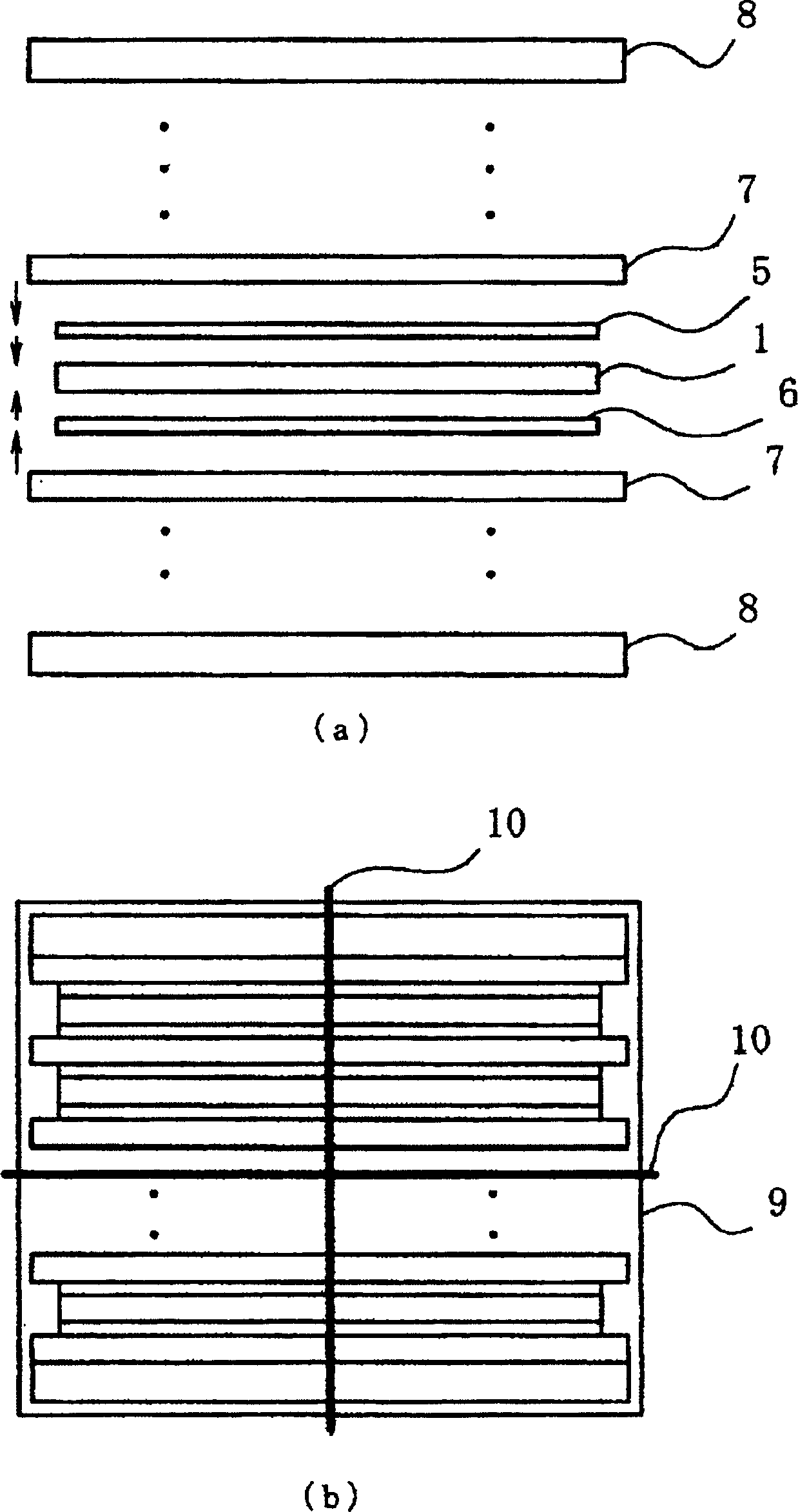
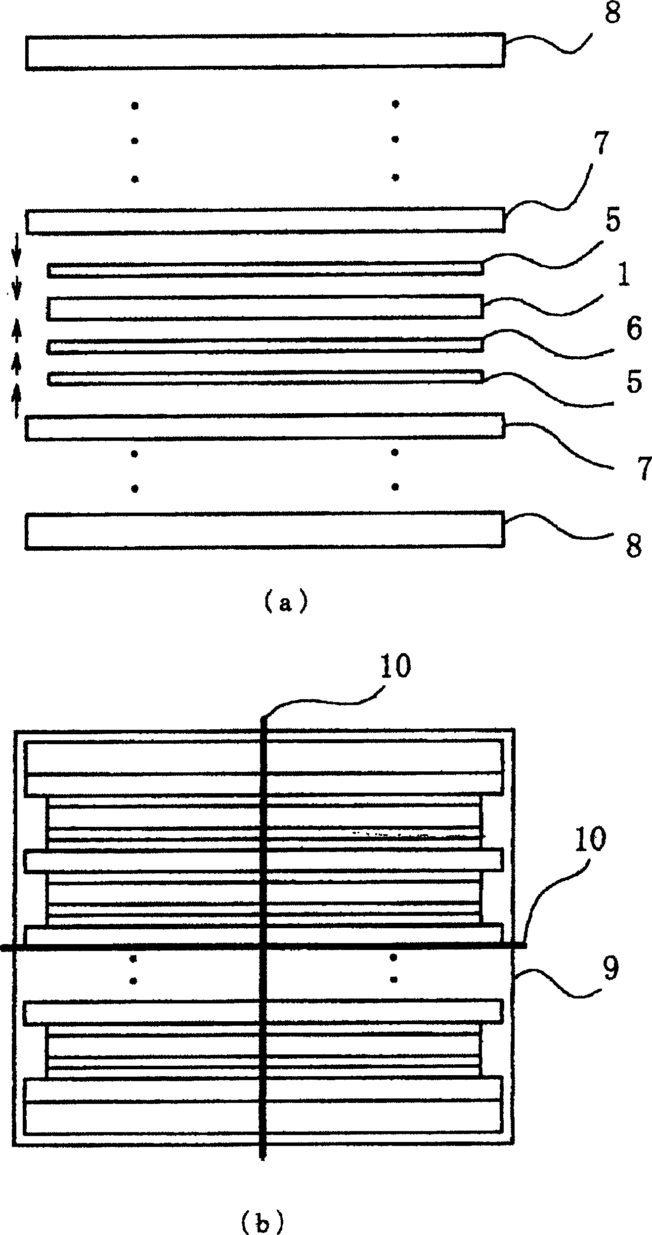
[0027] In the present invention, when the wafer is transported, a protective sheet for protecting the optical surface is attached to the entire upper surface of the wafer, a dicing tape is attached to the entire lower surface of the crystal, and a plurality of wafers are stacked and packaged with a buffer material in between. The subsequent process after the wafer is transported is to cut, clean, visually inspect, package, and ship the optical components obtained by dicing the wafer. Therefore, a dicing tape is attached to the lower surface of the wafer in advance to protect the lower surface of the wafer. In this state, the wafer is transported, and the wafer can be diced in this state directly after the transport. Therefore, the surface of the wafer is not in direct contact with the cushioning material, so damage or breakage due to vibration or impact during transportati...


PUM


Abstract

Provided is a highly reliable packaging element and also attain cost reduction in transportation when a wafer is transported. A fixation is carried out with rubber or tape 10 by sticking a protecting sheet 5 on the whole surface of the top face of the wafer 1, on the other hand, after sticking a dicing tape 6 on the whole surface of the undersurface of the wafer 1, by piling up the wafer 1 by inserting the first shock absorbing material 7 of the dimensions being fit to the size of the wafer 1 among these two or more wafers 1, finally, by disposing the second shock absorbing material 8 to both ends, and by wrapping the whole in a plastic bag 9. In accordance with this invention, since the protecting sheet 5 and the dicing tape 6 are stuck to both the ends of the wafer 1 and the whole surface is covered, the first shock absorbing material 7 which will be inserted between the wafers 1 is not needed to work into a frame shape, thus, the working costs of the first shock absorbing material 7 can be reduced sharply.

Description

technical field [0001] The present invention relates to a package for wafers, particularly a simple and highly reliable package for wafers required for transporting a wafer-shaped optical component as an intermediate product to another factory. Background technique [0002] As digital cameras, optical disc recording and reproducing devices, and the like become more popular and lower in price, the optical components used in them are also required to be lower in price, so optical component manufacturers are making unremitting efforts to reduce the manufacturing cost of optical components. [0003] As is well known, optical components are coated with optical films and the like in batches in the state of mother boards (hereinafter referred to as wafers), and then diced to separate them into individual optical components, just like semiconductor components. Then, after the cleaning process, visual inspection is carried out one by one, and the good and bad products are sorted out,...

Claims


Application Information

Patent Timeline
IPC IPC(8): B65D81/05B65D85/86
Inventor 松下洋久
Owner TOYO TSUSHINKI
Why Eureka
Try Eureka