Unlock instant, AI-driven research and patent intelligence for your innovation.

Mirror charge effect quantum cellular automation making method

A technology of quantum cell and production method, which is applied in the field of production of mirror-charge effect quantum cellular automata

Inactive Publication Date: 2006-11-22
INST OF SEMICONDUCTORS - CHINESE ACAD OF SCI
View PDF0 Cites 6 Cited by
  • Summary
  • Abstract
  • Description
  • Claims
  • Application Information

AI Technical Summary

Problems solved by technology

Although the structure scheme of image charge effect QCA has been proposed, so far there is no complete set of process methods for realizing image charge effect QCA

Method used


Image

  • Mirror charge effect quantum cellular automation making method
  • Mirror charge effect quantum cellular automation making method
  • Mirror charge effect quantum cellular automation making method

Examples


Embodiment

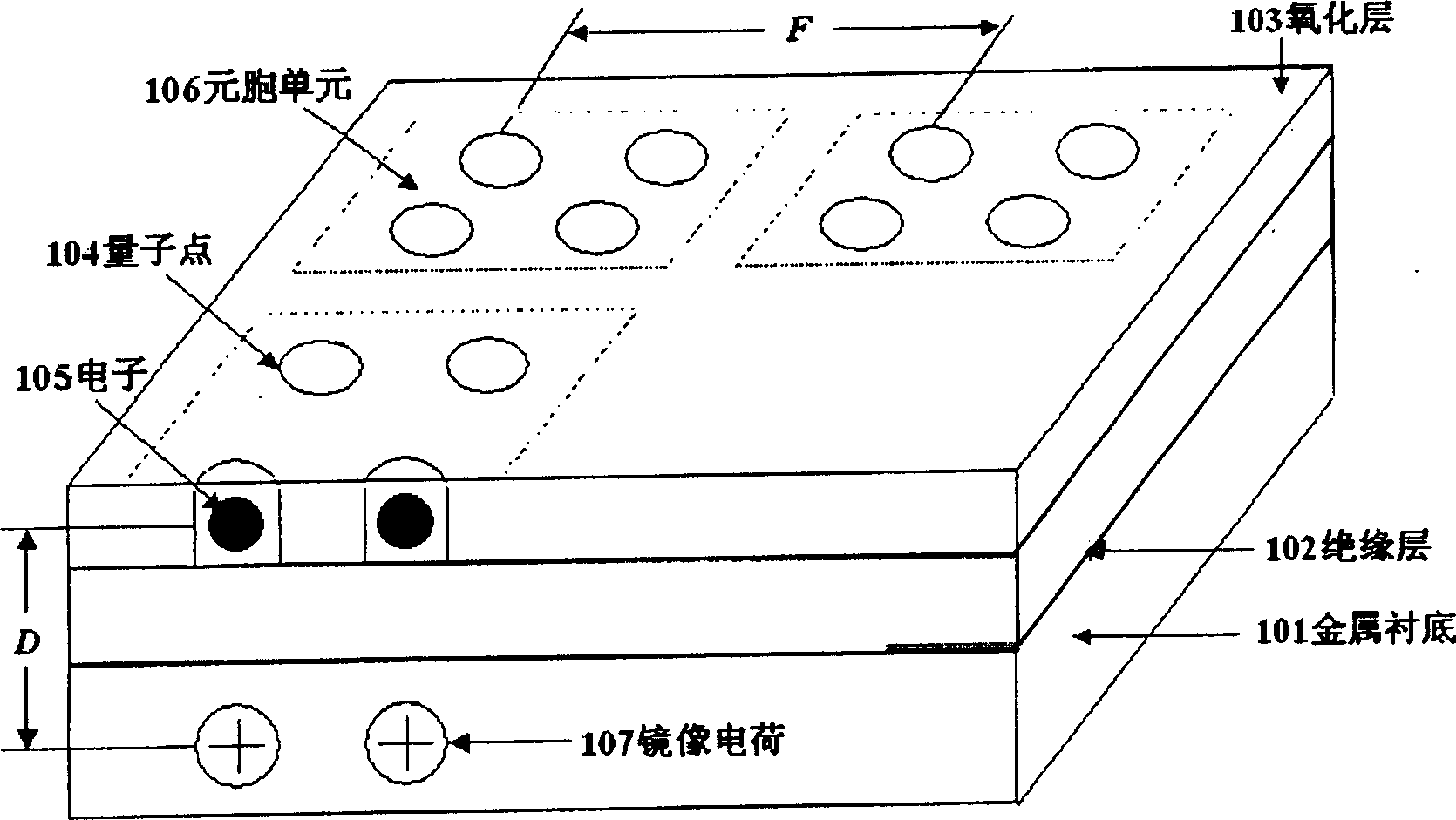
[0030] Please refer to FIG. 2 again. FIG. 2 shows a schematic diagram of the fabrication process of the mirror charge cellular automaton device. First, as shown in (a) in Figure 2, a silicon dioxide (SiO2) is deposited on the metal substrate 101 2 ) insulating layer 102, the thickness of the corresponding oxide layer can be obtained by adjusting parameters such as temperature and time according to the requirements of the image charge effect quantum cellular automaton device.

[0031] Then, as shown in Fig. 2(b), in SiO 2 The semiconductor layer 108 (Si wafer) can be bonded on the insulating layer 102 by a wafer bonding process. Then, the semiconductor layer 108 is thinned to a thickness below 100 nm by using a smartcut process, and the result shown in (c) of FIG. 2 is obtained.

[0032] Next, according to the structure of the image charge effect quantum cellular automaton device we want to obtain, the array of Si quantum dots 104 is formed, as shown in FIG. 2( d ). The arra...


PUM


Abstract

The invention discloses a preparing method of mirror-image charge effect quantum cell automat, which comprises the following steps: forming a thickness on the substrate to control the insulating layer; bonding semi-conductor on the substrate with insulating layer through chip bonding technology; utilizing intelligent cutting or grinding technology to reduce the thinness less than 100 nm; adopting etching technology to etch semi-conductor into quantum lattice array with multi-cell unit with four quantum points in one cell unit according to the need of quantum cell automat element and circuit; forming oxide layer around quantum point through oxidation and sediment technology; preparing mirror-image charge effect quantum cell automat with each cell containing two electrons; utilizing the scanning tunnel-piercing electrical mirror and atomic force microscope to inject extra electron; forming equal quantity of mirror-image positive charge on the substrate after the electron is injected.

Description

technical field [0001] The present invention designs a method for manufacturing a mirror image charge effect quantum cellular automaton, especially a method for forming an insulating layer with a controllable thickness such as two layers on a substrate with high conductivity such as a metal substrate or a highly doped semiconductor substrate. Silicon oxide (SiO 2 ), etc., use a wafer bonding process to bond semiconductor wafers such as silicon (Si) to a high-conductivity substrate with an insulating layer, use a thinning process to thin the semiconductor to a thickness below 100nm, and use etching According to the requirements of quantum cellular automaton devices and circuits, semiconductor thin layers are etched into quantum dots, and oxidation and deposition processes are used to form an oxide layer around the quantum dots to form a mirror charge effect quantum cellular automaton; It is suitable for the fabrication of image charge effect quantum cellular automata devices a...

Claims


Application Information

Patent Timeline
IPC IPC(8): H01L21/00B82B3/00
Inventor 汪艳贞吴南健
Owner INST OF SEMICONDUCTORS - CHINESE ACAD OF SCI