Photonic crystal-structural GaN-base blue LED structure and method for fabricating same
A technology of photonic crystals and blue light emission, which is applied in semiconductor devices, electrical components, circuits, etc.
- Summary
- Abstract
- Description
- Claims
- Application Information
AI Technical Summary
Problems solved by technology
Method used
Image

Examples
Embodiment
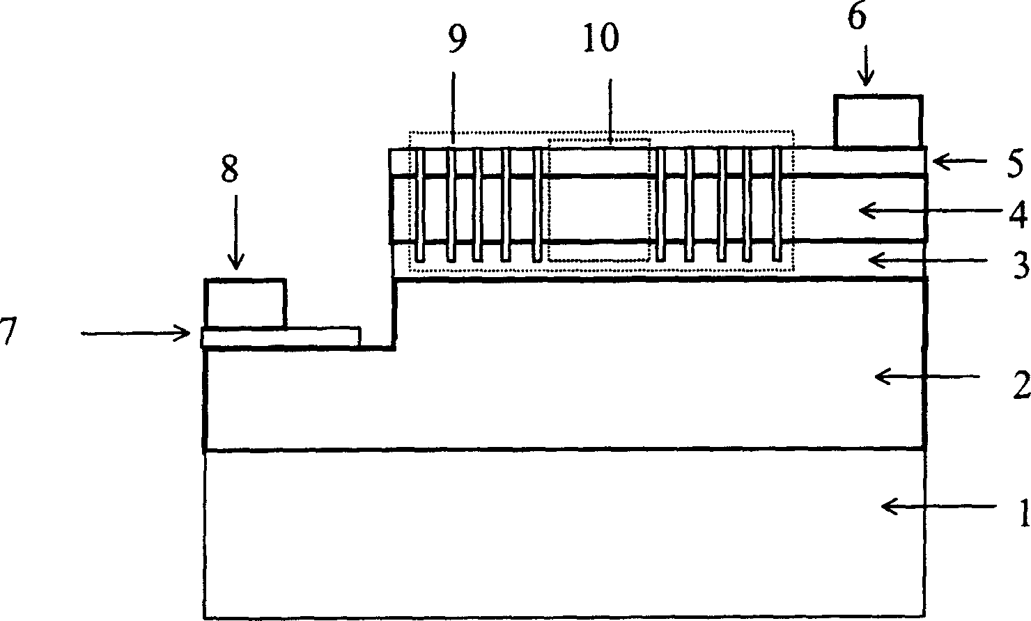
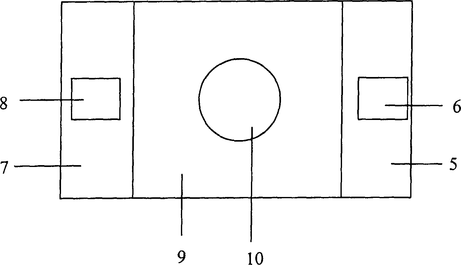
[0056] see figure 1 and figure 2 , the photonic crystal structure GaN-based blue light emitting diode structure includes a sapphire substrate 1; an N-type GaN layer 2, the N-type GaN layer 2 is directly grown on the sapphire substrate 1, and one side of the N-type GaN layer 2 There is a step etched on the plane to form a large plane and a small plane; a GaN material active layer 3, the GaN material active layer 3 is fabricated on the large plane on the N-type GaN layer 2; a P-type GaN layer 4. The P-type GaN layer 4 is made on the active layer 3; a P-type electrode 5 and a P-type pad 6, the P-type electrode 5 and the P-type pad 6 are laid on the P-type GaN layer 4; wherein the The electrode 5 described is a transparent electrode; the electrode 5 is laid on the upper side of the GaN layer 4 or laid on the entire GaN layer 4, and the electrode 5 is a square electrode or a ring electrode; an N-type electrode 7 and an N-type pad 8. The N-type electrode 7 and the N-type pad 8 ar...
PUM
 Abstract
Description
Claims
Application Information
 - R&D
- Intellectual Property
- Life Sciences
- Materials
- Tech Scout
- Unparalleled Data Quality
- Higher Quality Content
- 60% Fewer Hallucinations
Browse by: Latest US Patents, China's latest patents, Technical Efficacy Thesaurus, Application Domain, Technology Topic, Popular Technical Reports.
© 2025 PatSnap. All rights reserved.Legal|Privacy policy|Modern Slavery Act Transparency Statement|Sitemap|About US| Contact US: help@patsnap.com