Check patentability & draft patents in minutes with Patsnap Eureka AI!

Overcurrent detecting circuit and reference voltage generating circuit

A detection circuit and reference voltage technology, applied in the direction of adjusting electrical variables, control/regulation systems, instruments, etc., to achieve the effect of reducing power consumption

Inactive Publication Date: 2010-09-15
FUJI ELECTRIC CO LTD
View PDF5 Cites 0 Cited by
  • Summary
  • Abstract
  • Description
  • Claims
  • Application Information

AI Technical Summary

Problems solved by technology

[0017] In addition, in order to obtain sufficient response speed, perform Figure 4 The comparator COMP, which compares the drain potential Vd0 and Vd1 in the circuit, must also have a certain degree of power consumption (for example, 50μA)

Method used


Image

  • Overcurrent detecting circuit and reference voltage generating circuit
  • Overcurrent detecting circuit and reference voltage generating circuit
  • Overcurrent detecting circuit and reference voltage generating circuit

Examples


Embodiment Construction

[0057] Hereinafter, embodiments of the present invention will be described with reference to the drawings.

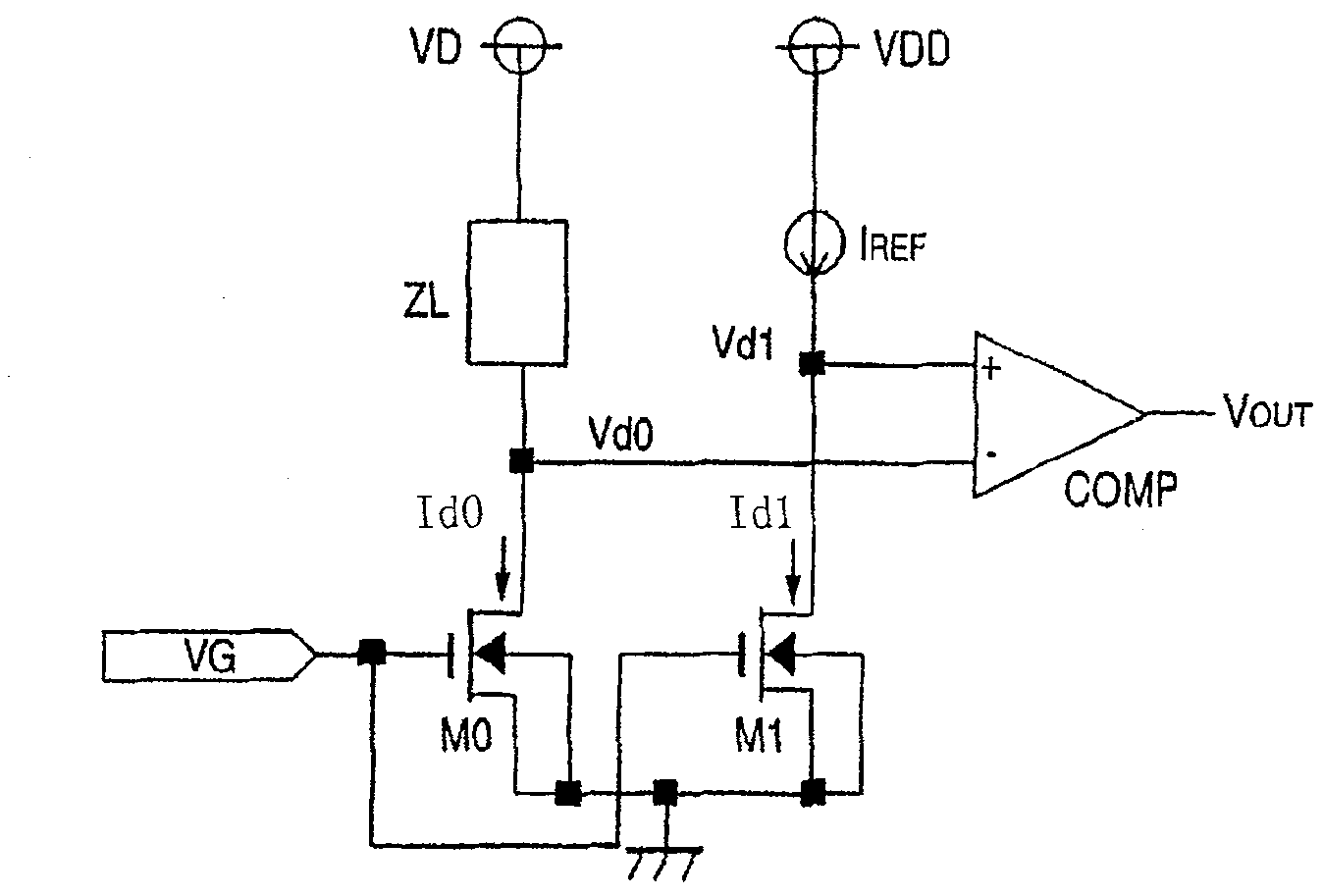
[0058] first of all, yes figure 1 To illustrate. This figure is a diagram showing a configuration of a reference voltage generating circuit embodying the present invention. The circuit is expressed with Figure 5 A circuit that operates in the same way as the circuit shown. That is, will Figure 4 The comparator COMP and the reference current Iref in the circuit shown are replaced by figure 1 circuit (except transistor M1), through the figure 1 An output amplifier is added to the output Vout of the circuit, and the same Figure 4 The circuit shown is the same overcurrent detection circuit.

[0059] right figure 1 The circuit is explained.

[0060] In this figure, M11 and M12 which are n-channel MOSFETs, and M13 and M14 which are p-channel MOSFETs constitute a differential amplifying section, and a bias current is supplied to this differential amplifying secti...


PUM


Abstract

The invention relates to an overcurrent detecting circuit which may includes a reference load (M1 as MOSFET) through which a reference current flows, generating a reference voltage corresonding to the reference current. A differential amplifier section (M11, M12, M13, M14) is included to amplify the difference in the potentials of two inputs. A bias current supplied by a constant current source (Ib) flows through the differential amplifier section. At least part of a bias current flows to the reference load. A detection voltage, corresponding to a current subject to overcurrent detection, is inputted to one of the two inputs of the differential amplifier section while the drain electrode of M10 entries to one of the two inputs potentials of the differential amplifier section. Thus, the invention can reduce the total current consumed by an electronic circuit.

Description

technical field [0001] The present invention relates to techniques for reducing power consumption in electronic circuits. Background technique [0002] Even in electronic circuits such as DC-DC converters, such as circuits used in portable devices, it is also urgently required to reduce power consumption. [0003] Circuits of conventional overcurrent detection circuits used in DC-DC converters and the like are shown in Figure 4 . However, the circuit shown in this figure is the circuit listed in Patent Document 1 as prior art. [0004] exist Figure 4 Among them, both M0 and M1 are n-channel MOSFETs (Metal Oxide Semiconductor Field Effect Transistors). Here, M0 is the main FET (Field Effect Transistor) of the output stage of the DC-DC converter, which drives the load ZL. The drain current Id0 of M0 flows from the power supply line VD to the ground line (reference potential) via the driven load ZL and M0. Further, M1 is a FET (Field Effect Transistor) functioning as a re...

Claims


Application Information

Patent Timeline
Patent Type & Authority Patents(China)
IPC IPC(8): G05F3/08
CPCG05F1/573
Inventor 山田耕平
Owner FUJI ELECTRIC CO LTD
Features
  • R&D
  • Intellectual Property
  • Life Sciences
  • Materials
  • Tech Scout
  • Unparalleled Data Quality
  • Higher Quality Content
  • 60% Fewer Hallucinations
Learn More