Check patentability & draft patents in minutes with Patsnap Eureka AI!

Low-power slew rate detector for edge rate control of an output power stage

a detector and output power stage technology, applied in pulse manipulation, pulse technique, instruments, etc., can solve the problems of d amplification, disturbance and interference of other circuits, and significant high-frequency content, and achieve the effect of simple circuit design and cost-effectiveness

Active Publication Date: 2018-08-07
NUVOTON
View PDF7 Cites 1 Cited by
  • Summary
  • Abstract
  • Description
  • Claims
  • Application Information

AI Technical Summary

Benefits of technology

The circuit effectively measures slew rates with reduced EMI interference and complexity, enabling cost-effective edge rate control in Class-D amplifiers, suitable for high voltage inputs and providing a digital output for processing.

Problems solved by technology

Such Pulse Width Modulated Waveform looks very much like a square wave and therefore, it has significant high-frequency content that can disturb and interfere with other circuits using radio frequencies much higher than the PWM frequency.
The disadvantage of class-D amplification lies in the high frequency switching noise that is produced by the switching.
This high frequency noise often resulted in EMI (Electronic-Magnetic Interference).
The fast edges on the signals OUTP and OUTM can cause electromagnetic interference (EMI).
Conventional methods have been proposed for determining the slew rate of a signal, but they are not satisfactory.
This circuit requires switches and voltage references at the input, which is not suitable for use with high voltage input signals and the switches can create glitches on the input signal.
Due to the trans-conductance amplifier the circuit is more complex and this added complexity and delay makes it slower, so it is not suitable for fast edge control.

Method used


Image

  • Low-power slew rate detector for edge rate control of an output power stage
  • Low-power slew rate detector for edge rate control of an output power stage
  • Low-power slew rate detector for edge rate control of an output power stage

Examples


Embodiment Construction

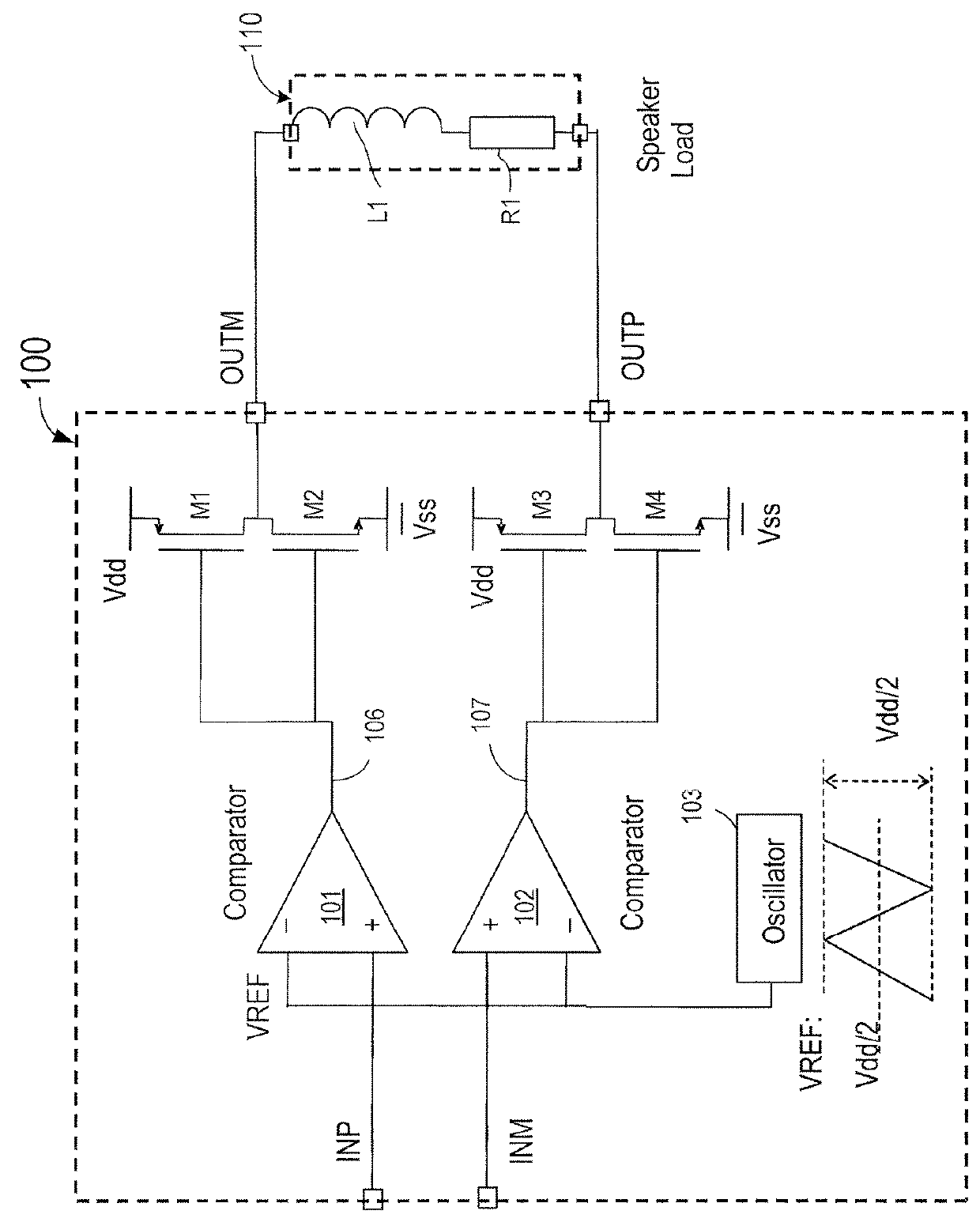
[0039]FIG. 4 is a circuit diagram illustrating a slew rate detection circuit according to an embodiment of the present invention. As shown in FIG. 4, a slew rate detection circuit 400 includes a capacitor C0 connected between an input signal VIN and a diode-connected first MOSFET (Metal-Oxide-Semiconductor Field Effect Transistor) M1. As noted in FIG. 4, capacitor C0 and MOSFET M1 are enclosed in a dashed block 410. The first MOSFET M1 is configured to carry a current during changes of an input signal, and the current is proportional to the slew rate of the input signal VIN.

[0040]In this embodiment, slew rate detection circuit 400 also includes a resistor R0 and a second MOSFET transistor (M2) coupled with the first MOSFET in series between a power terminal Vdd and a ground terminal GND. The first MOSFET has a drain terminal, a gate terminal, and a source terminal, wherein a first end of the resistor is coupled to the power terminal Vdd, a second end of the resistor R0 is coupled to...


PUM


Abstract

A circuit for determining a slew rate of an input signal includes a first MOSFET, a second MOSFET, and a resistor coupled in series between a ground terminal and a power terminal. The resistor is coupled between the power terminal and the second MOSFET, and the first MOSFET is coupled between the second MOSFET and the ground. The second MOSFET is coupled to a bias circuit to provide a bias current. The circuit also includes a capacitor having a first terminal and a second terminal, the first terminal coupled to the input signal and the second terminal coupled to the gate terminal and the drain terminal of the first MOSFET. A current flowing through the MOSFET during changes in the input signal represents a slew rate of the input signal.

Description

BACKGROUND OF THE INVENTION[0001]This invention relates to the field of semiconductor circuit technologies. More particularly, some embodiments of this invention are directed to low-power slew rate detector circuits. In some embodiments, the slew rate detection circuits are used in class-D output power stages for edge rate control. However, the circuits can be used in any applications where accurate slew rate detection is desired.[0002]In Class-D Audio amplifiers, the output signal is a Pulse Width Modulated (PWM) waveform, which drives the external speaker. Such Pulse Width Modulated Waveform looks very much like a square wave and therefore, it has significant high-frequency content that can disturb and interfere with other circuits using radio frequencies much higher than the PWM frequency. Below is shown a typical configuration of a first order Class-D stage and its input and output waveforms. FIG. 1 and FIG. 2.[0003]A class-D amplifier, sometimes known as a switching amplifier, ...

Claims


Application Information

Patent Timeline
Patent Type & Authority Patents(United States)
IPC IPC(8): H03K17/16H03K7/08G11C27/02H03K5/04H03K17/687G05F3/02H03K5/12H03F3/45H03K4/00
CPCH03K5/04H03K7/08G11C27/02G01R31/316H03F3/217H03F2200/03G11C27/024H03F3/2171H03F3/2175H03F2203/45248
Inventor HOLZMANN, PETER J.
Owner NUVOTON
Features
  • R&D
  • Intellectual Property
  • Life Sciences
  • Materials
  • Tech Scout
  • Unparalleled Data Quality
  • Higher Quality Content
  • 60% Fewer Hallucinations
Learn More