Check patentability & draft patents in minutes with Patsnap Eureka AI!

Electronic device

a technology of electronic devices and components, applied in the field of electronic devices, can solve problems such as increased process costs

Inactive Publication Date: 2018-08-14
SAMSUNG ELECTRONICS CO LTD
View PDF5 Cites 0 Cited by
  • Summary
  • Abstract
  • Description
  • Claims
  • Application Information

AI Technical Summary

Benefits of technology

This configuration enables efficient electrical signal exchange between active chips, reduces process costs, and allows for more flexible chip design by utilizing dummy chips to manage TSV connections, improving the integration level and reducing the risk of chip damage.

Problems solved by technology

Moreover, when penetrating the semiconductor chip, the semiconductor chip may be damaged, resulting in increased process cost.

Method used


Image

  • Electronic device
  • Electronic device
  • Electronic device

Examples


Embodiment Construction

[0014]Hereinafter, exemplary embodiments of the present invention are described in detail with reference to the accompanying drawings. The same or like reference numbers are used throughout the drawings to refer to the same or like parts. The views in the drawings may be schematic views only, and may not be to scale or correctly proportioned. Detailed descriptions of well-known functions and structures incorporated herein may be omitted to avoid obscuring the subject matter of the present invention.

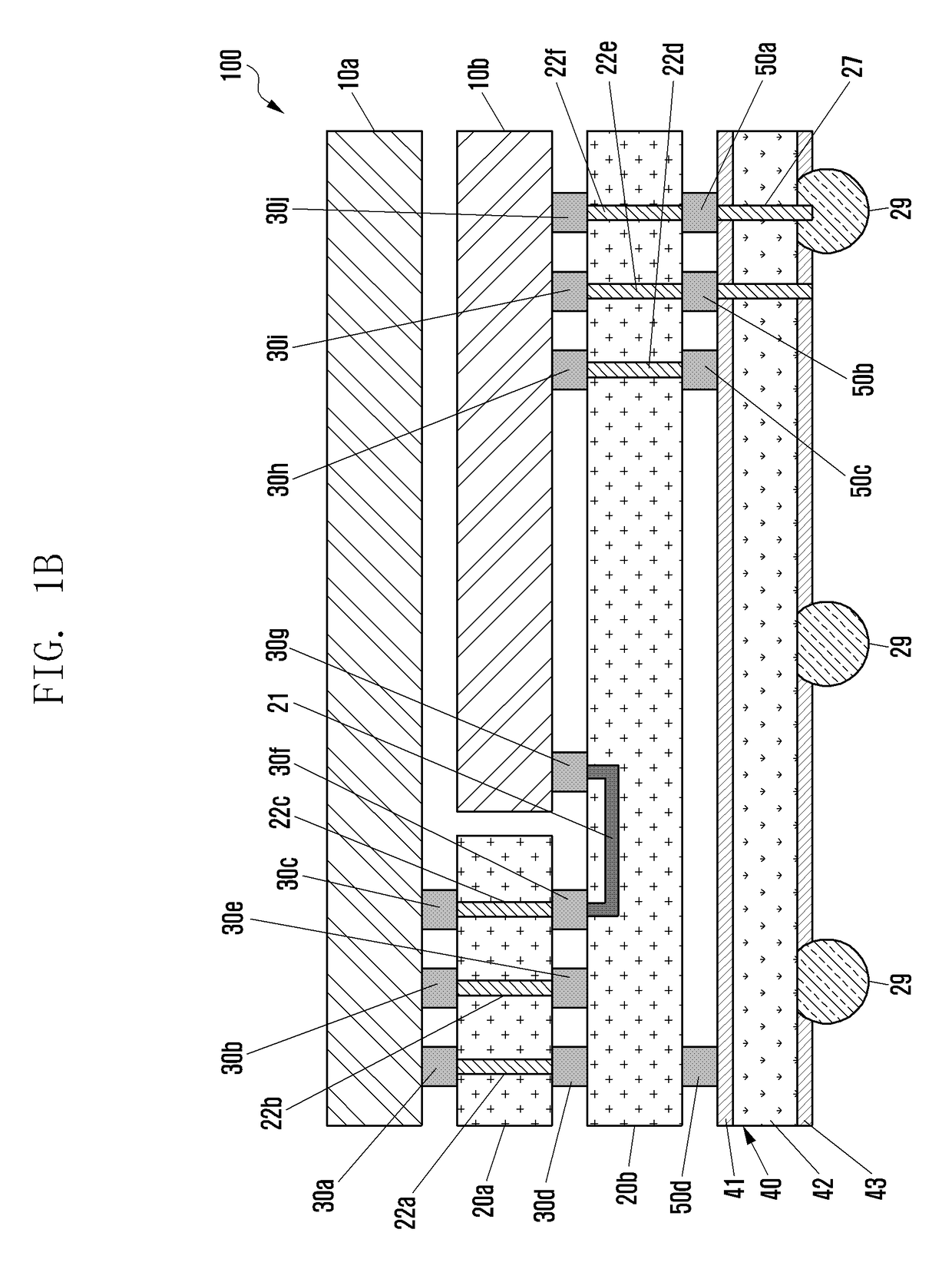
[0015]FIGS. 1A and 1B are cross-sectional views illustrating a semiconductor device, 10, according to an example. For clarity of illustration, FIG. 1A shows the device without a substrate whereas FIG. 1B shows the device with a substrate. Semiconductor device 100 can also be considered an electronic device.

[0016]As shown in FIGS. 1A and 1B, semiconductor device 10 includes a plurality of semiconductor chips 10a, 10b, 20a, and 20b that exchange an electrical signal amongst one another. Chi...


PUM


Abstract

A semiconductor device and electronic device comprising the same includes at least one dummy chip having at least one Through Silicon Via (TSV), and at least one active chip connected to the at least one dummy chip. The at least one active chip exchanges an electrical signal through the at least one TSV. The at least one active chip may be a memory chip and a non-memory chip in a vertically stacked (3D) configuration, connected through an electrical path that includes the TSV of the dummy chip. Embodiments may include multiple memory chips and dummy chips.

Description

CLAIM OF PRIORITY[0001]This application claims the benefit under 35 U.S.C. § 119(a) of a Korean patent application filed on Oct. 18, 2013 in the Korean Intellectual Property Office and assigned Serial No. 10-2013-0124935, the entire disclosure of which is hereby incorporated by reference.BACKGROUND[0002]Field[0003]The present disclosure relates to an electronic device, and more particularly, to a semiconductor device including a plurality of chips and an electronic device including the semiconductor device.[0004]Description of the Related Art[0005]Recent technological advances have continued to increase capacity and speed of semiconductor chips and Integrated Circuits (IC) used in most electronic devices. As large capacity semiconductor chips and ICs have been mounted within small spaces, various attempts for efficiently driving them have been proposed.[0006]In order to enhance an integration level of semiconductor devices, so-called three-dimensional (3D) integration / packaging tech...

Claims


Application Information

Patent Timeline
Patent Type & Authority Patents(United States)
IPC IPC(8): H01L23/48H01L23/14H01L23/00H01L25/065H01L23/538H01L23/498
CPCH01L24/16H01L23/147H01L23/5384H01L23/5385H01L25/065H01L2924/37001H01L2924/15311H01L2924/15192H01L23/49816H01L2224/131H01L2224/16146H01L2224/16227H01L2224/16235H01L2224/81815H01L2924/00014H01L2924/014H01L2225/06527H01L25/0657H01L25/18H01L2225/06517H01L2225/06562H01L2225/06572H01L2225/06548H01L23/12H01L23/48
Inventor KIM, SEIJIN
Owner SAMSUNG ELECTRONICS CO LTD
Features
  • R&D
  • Intellectual Property
  • Life Sciences
  • Materials
  • Tech Scout
  • Unparalleled Data Quality
  • Higher Quality Content
  • 60% Fewer Hallucinations
Learn More