Supercharge Your Innovation With Domain-Expert AI Agents!

Active matrix display device and method of driving same

a display device and active matrix technology, applied in static indicating devices, non-linear optics, instruments, etc., can solve the problems of not being able to represent image data at a level of detail, and the transmission of two regions does not provide an increase in display resolution, so as to achieve the effect of increasing resolution

Active Publication Date: 2018-11-06
SHARP KK
View PDF17 Cites 0 Cited by
  • Summary
  • Abstract
  • Description
  • Claims
  • Application Information

AI Technical Summary

Benefits of technology

The patent text describes a method for supplying capacitor line voltages to a display screen to improve resolution. By varying the relationship between the capacitor line voltages, the relative transmissivity of the sub-pixels can be adjusted, resulting in higher resolution. This approach overcomes limitations in previous methods that fixed the relative transmissivity of the sub-pixels over a frame.

Problems solved by technology

One potential limitation of the driving methods described in U.S. Pat. No. 7,079,214 is that, although a different transmittance may be produced by the two pixel regions, their relative transmittance has a fixed relationship.
Therefore if region A of one pixel of the row is made brighter than region B, then this is true for all pixels in the row (driven with the same voltage polarity, the relative brightness while still fixed being inverted for pixels driven with the opposite polarity), and the capability of providing different transmittance from the two regions does not provide an increase in display resolution.
Neither the degree of difference in brightness between the two regions, nor which region is the brighter can be varied from pixel to pixel, so it is not possible to represent image data at a level of detail finer than the pixel array of the panel.

Method used


Image

  • Active matrix display device and method of driving same
  • Active matrix display device and method of driving same
  • Active matrix display device and method of driving same

Examples


Embodiment Construction

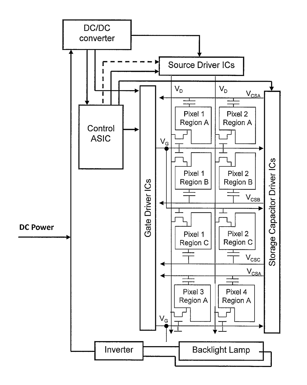
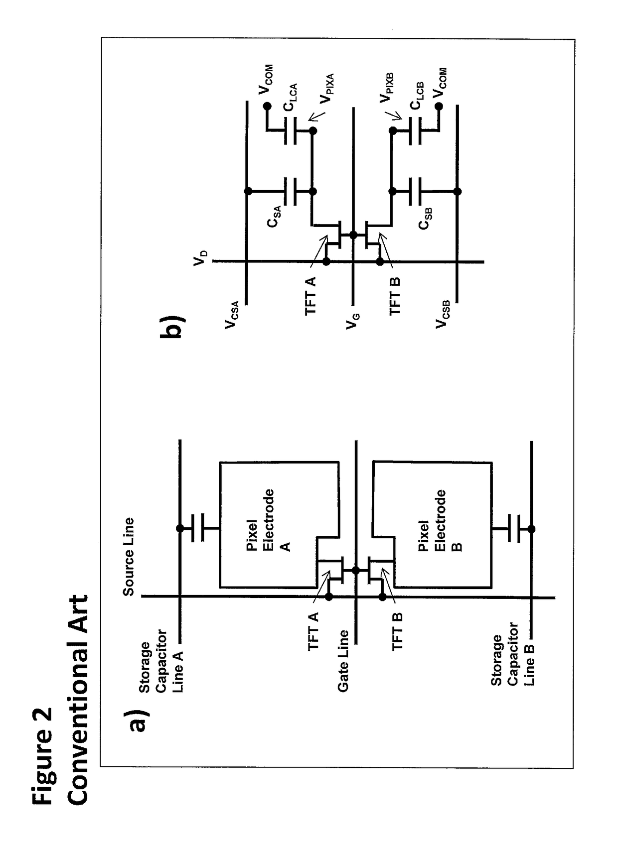
[0055]It is therefore desirable to provide an active matrix LCD display, with MPD pixel architecture generally as shown in FIGS. 2(a) and 2(b), and in which the root mean squared voltage applied across each of the two or more regions within a single pixel over a number of display refresh periods, and therefore the brightness produced by each of the regions, is controllable with a degree of independence, thereby increasing the resolution of the LCD panel without any addition or modification to the number of pixels or the electronic components comprising each pixel.

[0056]In a principal embodiment of this invention an active matrix LCD display, with MPD pixel architecture is provided with control electronics which may consist of a control unit and driver integrated circuits (ICs) as shown in FIG. 4. Each of Pixel 1, Pixel 2 etc. is a single-coloured pixel—the display may comprise groups of pixels of three or more different colours arranged to give composite white pixels, but the invent...


PUM

PropertyMeasurementUnit
rms voltageaaaaaaaaaa

Abstract

An active matrix LCD display of the multi-pixel drive (MPD) type, in which a pixel comprises a plurality of sub-pixels with each sub-pixel of a pixel being associated with a respective storage capacitor address lines so that the voltage applied across an individual sub-pixel depends on both the signal voltage and the voltage applied to the associated storage capacitor address line, is driven such that the relationship between at least a first one of the capacitor line voltages and a second one of the capacitor line in a first display refresh period of the frame is different to the relationship between the first of the capacitor line voltages and the second of the capacitor line voltages in a second display refresh period of the frame. This allows the root-mean-square (RMS) voltage applied over the frame across a first of the sub-pixels to be controlled at least partially independently of the RMS voltage applied over the frame across a second of the sub-pixels, thereby providing increased resolution.

Description

TECHNICAL FIELD[0001]The invention relates to a display device and, more particularly, an LCD display of the multi-pixel drive (MPD) type. Further, the invention relates to a method of driving such a display device.BACKGROUND ART[0002]In an active matrix liquid crystal display (LCD), an image is produced by controlling the light transmittance of a two-dimensional array of discrete image elements (pixels), via the conversion of digital image data, consisting of a data value for each pixel of the image, into analogue voltages with values dependent on that data, and direction of those voltages to each pixel electrode in the array via an active matrix of source data lines, gate lines and thin film transistor (TFT) switching elements. This type of arrangement is illustrated in FIG. 1 (from Ernst Lueder, Liquid Crystal Displays, Wiley and Sons Ltd, 2001, and more fully described in that publication). In such an arrangement each pixel may be defined as each separate electrode area in which...

Claims


Application Information

Patent Timeline
Patent Type & Authority Patents(United States)
IPC IPC(8): G09G3/36G02F1/1362
CPCG09G3/3696G09G3/3607G09G3/3648G02F1/13624G09G2310/0235G02F2201/52G09G2300/0452G09G2300/0876G02F1/136213G09G3/3655G09G2300/0443
Inventor GASS, PAUL ANTONYBROUGHTON, BENJAMIN JOHNWALTON, EMMA JAYNEBROWN, CHRISTOPHER JAMES
Owner SHARP KK
Features
  • R&D
  • Intellectual Property
  • Life Sciences
  • Materials
  • Tech Scout
  • Unparalleled Data Quality
  • Higher Quality Content
  • 60% Fewer Hallucinations
Learn More