Check patentability & draft patents in minutes with Patsnap Eureka AI!

Organic photoelectronic device and image sensor

an image sensor and photoelectronic technology, applied in the direction of organic semiconductor devices, radio frequency controlled devices, organic chemistry, etc., can solve problems such as deterioration of sensitivity, and achieve the effect of improving efficiency and thermal stability

Active Publication Date: 2019-04-09
SAMSUNG ELECTRONICS CO LTD
View PDF39 Cites 11 Cited by
  • Summary
  • Abstract
  • Description
  • Claims
  • Application Information

AI Technical Summary

Benefits of technology

The organic photoelectronic device selectively absorbs light in the green wavelength region, enhancing sensitivity and thermal stability, and when integrated into an image sensor, it improves external quantum efficiency and maintains performance even after thermal stress.

Problems solved by technology

Currently, a silicon photodiode is widely used, but presents the disadvantage of deteriorated sensitivity because of a small absorption area due to small pixels.

Method used

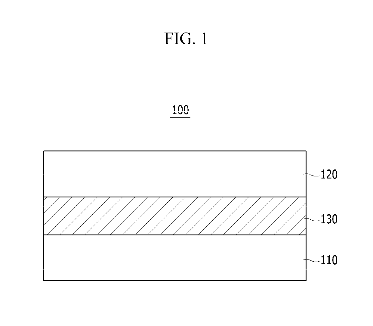
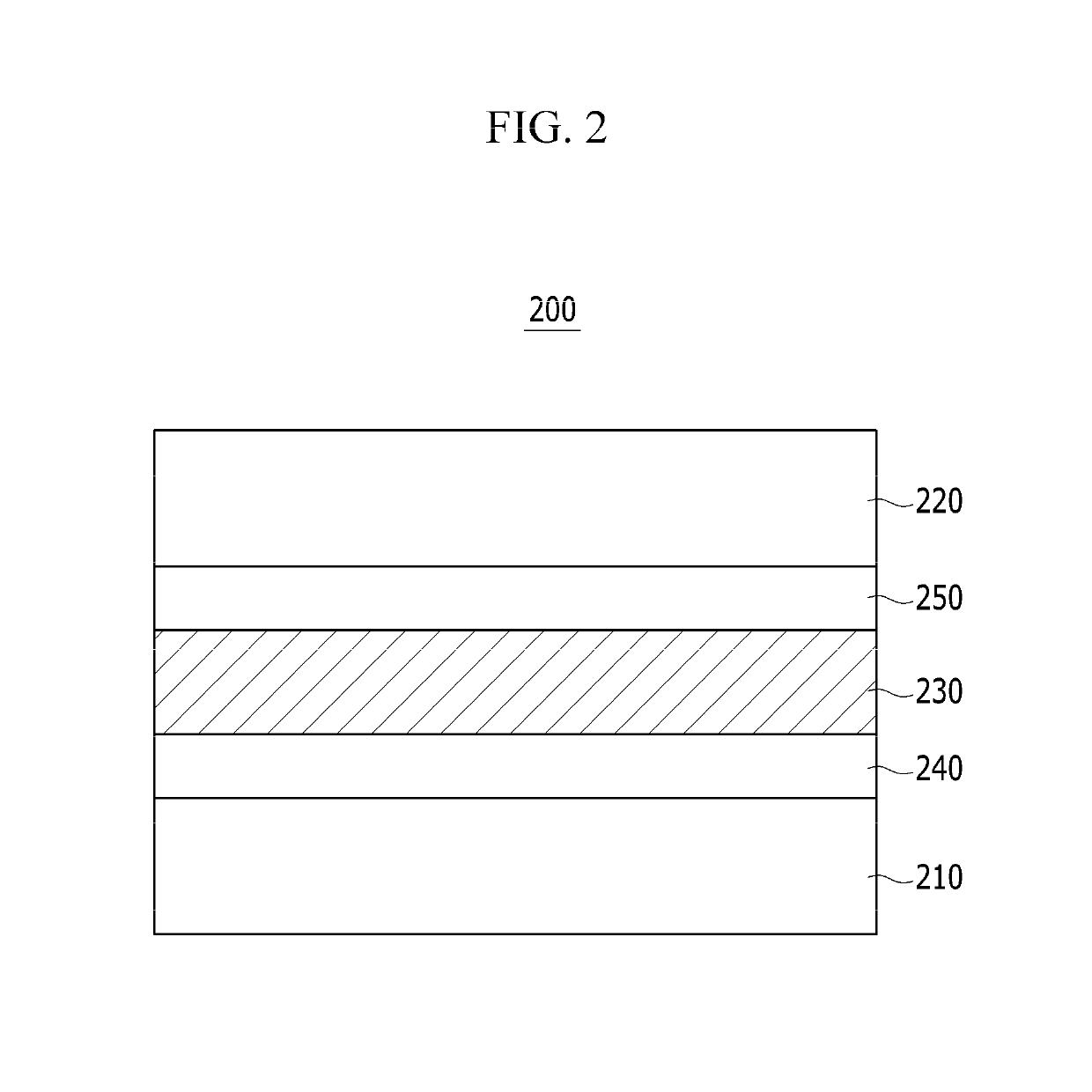
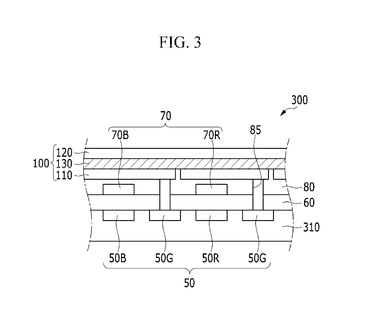

Image

  • Organic photoelectronic device and image sensor
  • Organic photoelectronic device and image sensor
  • Organic photoelectronic device and image sensor

Examples


synthesis example

Synthesis Example 1

[0149]

[0150]

[0151]1 mmol of 2,9-dimethylquinacridone (Chemieliva Pharmaceutical Co., Ltd.) is dissolved in 40 ml of dimethyl formamide (DMF). Subsequently 2.5 mmol of NaH (60% oil dispersion) is added to the mixture at 0° C. The obtained mixture is then agitated at 60° C. for 30 minutes and cooled down to room temperature while maintaining agitation. Subsequently, 2.5 mmol of iodomethane is added to the mixture, and the obtained mixture is additionally agitated at 60° C. for 18 hours and supplied with water. The obtained mixture is filtered to collect a solid, and the solid is completely washed, obtaining a reddish orange solid. The solid is filtered through silica gel column chromatography and recrystallized twice by using hexane, obtaining a compound represented by the above Chemical Formula 1aa. The compound has a boiling point of 325° C., and its yield is 74%.

[0152]1H-NMR and mass data of the compound is as follows.

[0153]1H-NMR (CDCl3, 300 MHz): δ8.75 (s, 2H),...

synthesis example 2

[0155]

[0156]

[0157]A compound represented by the above Chemical Formula 1ab is synthesized according to the same method as Synthesis Example 1, except for using 2.5 mmol of 1-iodooctane instead of the iodomethane. The compound has a boiling point of 230° C.

[0158]1H-NMR and mass data of the compound is as follows.

[0159]1H-NMR (CDCl3, 300 MHz): δ8.72 (s, 2H), δ8.33 (s, 2H), δ7.54 (d, 2H, J=9.0 Hz), δ7.42 (d, 2H, J=9.0 Hz), δ4.49 (m, 4H), δ2.48 (s, 6H), δ1.98 (m, 4H), δ1.46 (m, 20H), δ0.90 (m, 6H).

[0160]MALDI-TOF mass: 565.02 (m / z).

[0161]Elemental analysis: Calculated for C38H48N2O2: C, 80.81%; H, 8.57%; N, 4.96%; 0, 5.67%. Found: C, 80.86%; H, 8.65%; N, 4.95%; 0, 5.54%.

synthesis example 3

[0162]A compound represented by the following Chemical Formula 2a is prepared (sublimed grade, Luminescence Technology Corp.)

[0163]


PUM


Abstract

Disclosed are an organic photoelectronic device including a first electrode and a second electrode facing each other and an active layer interposed between the first electrode and the second electrode, wherein the active layer includes a p-type semiconductor compound represented by the formula C22R1—R12O2N2 and an n-type semiconductor compound having a maximum absorption peak at a wavelength region of about 500 nm to about 600 nm, and an image sensor including the organic photoelectronic device.

Description

[0001]This application claims priority from Korean Patent Application No. 10-2013-0151095, filed in the Korean Intellectual Property Office on Dec. 6, 2013, the entire contents of which are incorporated herein by reference.BACKGROUND[0002]1. Field[0003]Example embodiments of an organic photoelectronic device and of an image sensor including the same are disclosed.[0004]2. Description of the Related Art[0005]A photoelectronic device converts light into an electrical signal using photoelectronic effects, and may include a photodiode, a phototransistor, and the like, and may be applied to an image sensor, a solar cell, and the like.[0006]An image sensor including a photodiode typically requires high resolution and thus a small pixel size. Currently, a silicon photodiode is widely used, but presents the disadvantage of deteriorated sensitivity because of a small absorption area due to small pixels. Accordingly, an organic material that is capable of replacing silicon has been researched...

Claims


Application Information

Patent Timeline
Patent Type & Authority Patents(United States)
IPC IPC(8): H01L27/30H01L51/00H01L51/42H10K99/00
CPCH01L51/0072H01L27/307H01L2251/308H01L51/008H01L51/4253H01L51/001Y02E10/549H10K39/32H10K71/164H10K85/322H10K85/6572H10K30/30H10K2102/103C07D471/04H01L27/146
Inventor LIM, SEON-JEONGPARK, KYUNG BAELEEM, DONG-SEOKHAN, MOON GYUKIM, KYU SIKRO, TAKKYUNLEE, KWANG HEEJIN, YONG WANHEO, CHUL JOON
Owner SAMSUNG ELECTRONICS CO LTD
Features
  • R&D
  • Intellectual Property
  • Life Sciences
  • Materials
  • Tech Scout
  • Unparalleled Data Quality
  • Higher Quality Content
  • 60% Fewer Hallucinations
Learn More