Supercharge Your Innovation With Domain-Expert AI Agents!

Quantum dot electroluminescent device and method of manufacturing the same

a quantum dot electroluminescent and electroluminescent technology, applied in the field of electroluminescent, can solve the problems of reducing serious imbalance between electrons and holes, etc., and achieve the effect of improving the luminescent efficiency of the device and reducing the energy barrier of the holes

Active Publication Date: 2019-12-24
TCL CHINA STAR OPTOELECTRONICS TECH CO LTD
View PDF10 Cites 0 Cited by
  • Summary
  • Abstract
  • Description
  • Claims
  • Application Information

AI Technical Summary

Benefits of technology

The gradient doping effect in the multi-layer hole and electron transmission layers improves luminescent efficiency by reducing the energy barrier for hole injection, leading to improved light emission performance.

Problems solved by technology

However, in the QLED design, since the QD material has a deeper HOMO (highest occupied molecular orbital) energy level, there is a larger energy barrier (>1 eV) between a hole transmission material and the HOMO energy level of the QD material, while an electron injection hardly has the energy barrier, thereby causing a serious imbalance between the electrons and the holes, and reducing the luminescent efficiency of the device.

Method used


Image

  • Quantum dot electroluminescent device and method of manufacturing the same
  • Quantum dot electroluminescent device and method of manufacturing the same
  • Quantum dot electroluminescent device and method of manufacturing the same

Examples


first embodiment

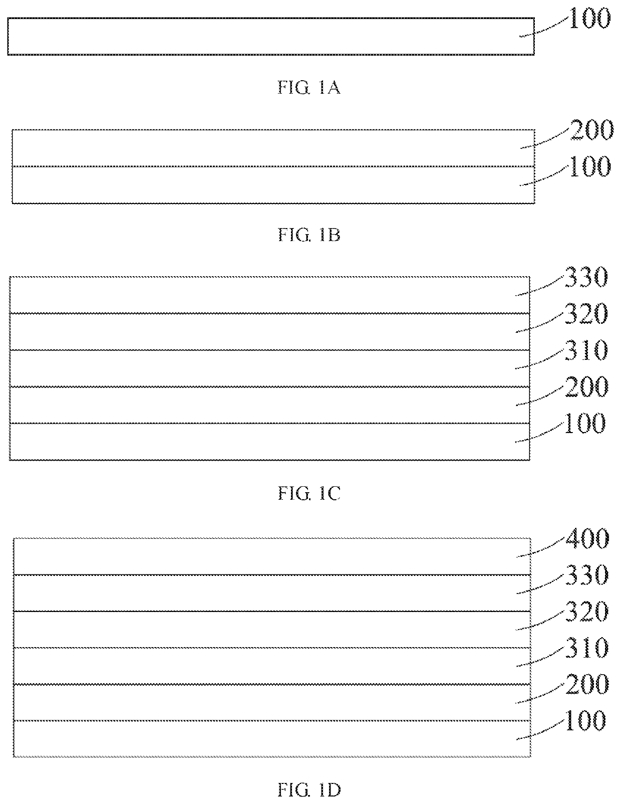
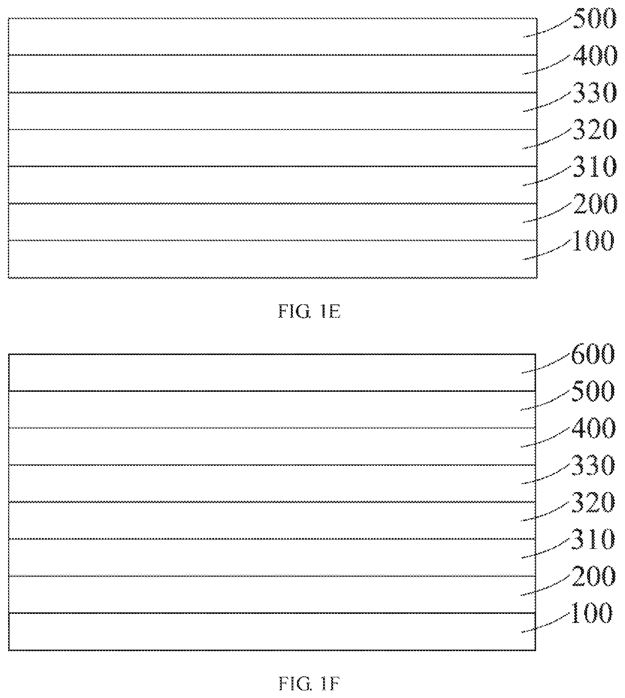
[0021]FIGS. 1A to 1F are process diagrams of a method of manufacturing a quantum dot electroluminescent device according to the present disclosure.

[0022]The method of manufacturing the quantum dot electroluminescent device according to the first embodiment of the present disclosure includes the following steps.

[0023]Step 1: providing a substrate 100 by referring to FIG. 1A. The substrate 100 may be a hard substrate, such as a transparent hard glass substrate or a transparent hard resin substrate, and may also be a flexible substrate here.

[0024]Step 2: manufacturing and forming an anode 200 on the substrate by referring to FIG. 1B. Here, the anode 200 may be transparent or semi-transparent or non-transparent, which is determined according to a direction of light emission. If the light is emitted from a side of a cathode 600, the anode 200 is non-transparent and may reflect the light; and if the light is emitted from a side of the anode 200, the anode 200 is transparent or semi-transp...

second embodiment

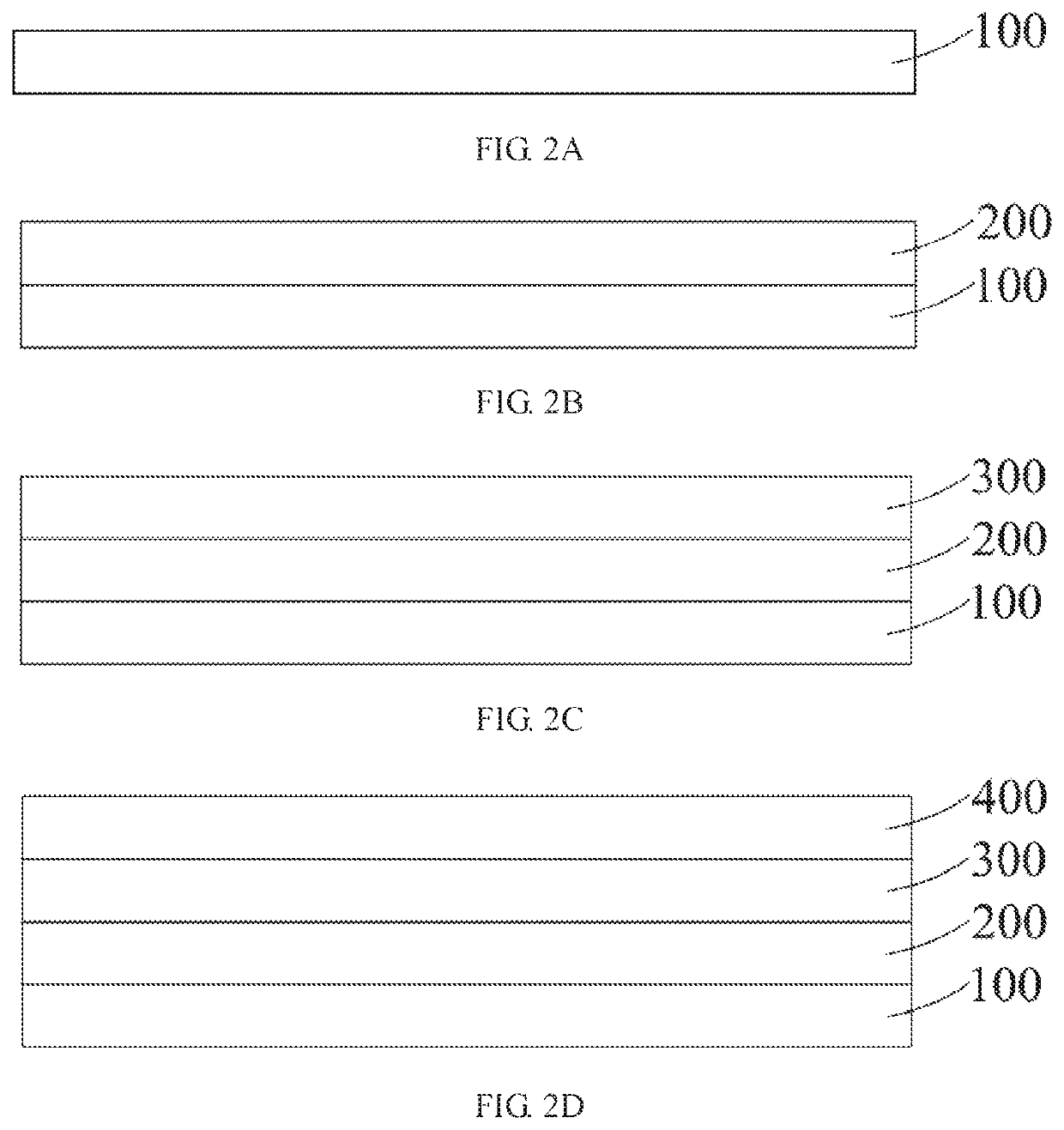
[0032]FIGS. 2A to 2F are process diagrams of a method of manufacturing a quantum dot electroluminescent device according to the present disclosure.

[0033]The method of manufacturing the quantum dot electroluminescent device according to the second embodiment of the present disclosure includes as follows.

[0034]Step 1: providing a substrate 100 by referring to FIG. 2A. The substrate 100 may be a hard substrate, such as a transparent hard glass substrate or a transparent hard resin substrate, and may also be a flexible substrate here.

[0035]Step 2: manufacturing and forming an anode 200 on the substrate by referring to FIG. 2B. Here, the anode 200 may be transparent or semi-transparent or non-transparent, which is determined according to a direction of light emission. If the light is emitted from a side of a cathode 600, the anode 200 is non-transparent and may reflect the light; and if the light is emitted from a side of the anode 200, the anode 200 is transparent or semi-transparent.

[0...

third embodiment

[0041]FIGS. 3A to 3F are process diagrams of a method of manufacturing a quantum dot electroluminescent device according to the present disclosure.

[0042]The method of manufacturing the quantum dot electroluminescent device according to the third embodiment of the present disclosure includes as follows.

[0043]Step 1: providing a substrate 100 by referring to FIG. 3A. The substrate 100 may be a hard substrate, such as a transparent hard glass substrate or a transparent hard resin substrate, and may also be a flexible substrate here.

[0044]Step 2: manufacturing and forming an anode 200 on the substrate by referring to FIG. 3B. The anode 200 may be transparent or semi-transparent or non-transparent, which is determined according to a direction of light emission here. If the light is emitted from a side of a cathode 600, the anode 200 is non-transparent and may reflect the light; and if the light is emitted from a side of the anode 200, the anode 200 is transparent or semi-transparent.

[004...


PUM


Abstract

The present disclosure provides a quantum dot electroluminescent device, which includes: a substrate; an anode disposed on the substrate; a hole transmission layer disposed on the anode; a quantum dot luminescent layer disposed on the hole transmission layer; an electron transmission layer disposed on the quantum dot luminescent layer; and a cathode disposed on the electron transmission layer, wherein the hole transmission layer is a P-type doped hole transmission layer and / or the electron transmission layer is a N-type doped electron transmission layer. The present disclosure further provides a method of manufacturing the quantum dot electroluminescent device. The present disclosure causes degrees of curvature of interfacial energy bands to be different by forming a gradient doping effect in a multi-layer hole transmission layer, so as to form a gradient energy level, that is, the HOMO energy level deepens in order from the anode to the quantum dot luminescent layer, thereby reducing the energy barrier of the holes being injected from the anode to the quantum dot luminescent layer to improve the luminescent efficiency of the device.

Description

CROSS-REFERENCES TO RELATED APPLICATIONS[0001]This application is a U.S. national phase application, pursuant to 35 U.S.C. § 371, of PCT / CN2017 / 092711, filed Jul. 13, 2017, designating the United States, which claims priority to Chinese Application No. 201710505477.9, filed Jun. 28, 2017. The entire contents of the aforementioned patent applications are incorporated herein by this reference.TECHNICAL FIELD[0002]The present disclosure belongs to an electroluminescent technical field, and specifically, relates to a quantum dot electroluminescent device and a method of manufacturing the same.BACKGROUND ART[0003]A quantum dot electroluminescent device (QLED), like an organic light emitting device (OLED), may actively emit light and has advantages of a fast response speed, wide angle of view, light weight, low power consumption and the like; meanwhile, compared with the OLED, the QLED has a higher color purity and may implement a wider color gamut when being applied to a display device. ...

Claims


Application Information

Patent Timeline
Patent Type & Authority Patents(United States)
IPC IPC(8): H01L51/50H01L51/56
CPCH01L51/508H01L51/56H01L51/5064H01L51/502H01L51/5004H10K50/11H10K2101/40H10K50/115H10K50/156H10K50/166H10K71/00H10K71/30H10K50/155H10K50/165H10K2101/80
Inventor ZHOU, KAIFENG
Owner TCL CHINA STAR OPTOELECTRONICS TECH CO LTD
Features
  • R&D
  • Intellectual Property
  • Life Sciences
  • Materials
  • Tech Scout
  • Unparalleled Data Quality
  • Higher Quality Content
  • 60% Fewer Hallucinations
Learn More