Check patentability & draft patents in minutes with Patsnap Eureka AI!

Capacitor structure and semiconductor device including the same

a capacitor and capacitor technology, applied in the direction of capacitors, semiconductor devices, semiconductor/solid-state device details, etc., can solve the problem of difficulty in increasing the capacitance per unit area of capacitors

Active Publication Date: 2019-12-31
SAMSUNG ELECTRONICS CO LTD
View PDF10 Cites 0 Cited by
  • Summary
  • Abstract
  • Description
  • Claims
  • Application Information

AI Technical Summary

Benefits of technology

This design enhances the reliability and productivity of semiconductor devices by preventing potential differences between conductive pattern layers and electrode pads, thereby reducing the risk of capacitor breakdown and current leakage, while maintaining a simple and cost-effective manufacturing process.

Problems solved by technology

However, since there is a limit in selecting a dielectric material constituting a capacitor, there is a difficulty in increasing capacitance per unit area of a capacitor.

Method used


Image

  • Capacitor structure and semiconductor device including the same
  • Capacitor structure and semiconductor device including the same
  • Capacitor structure and semiconductor device including the same

Examples


Embodiment Construction

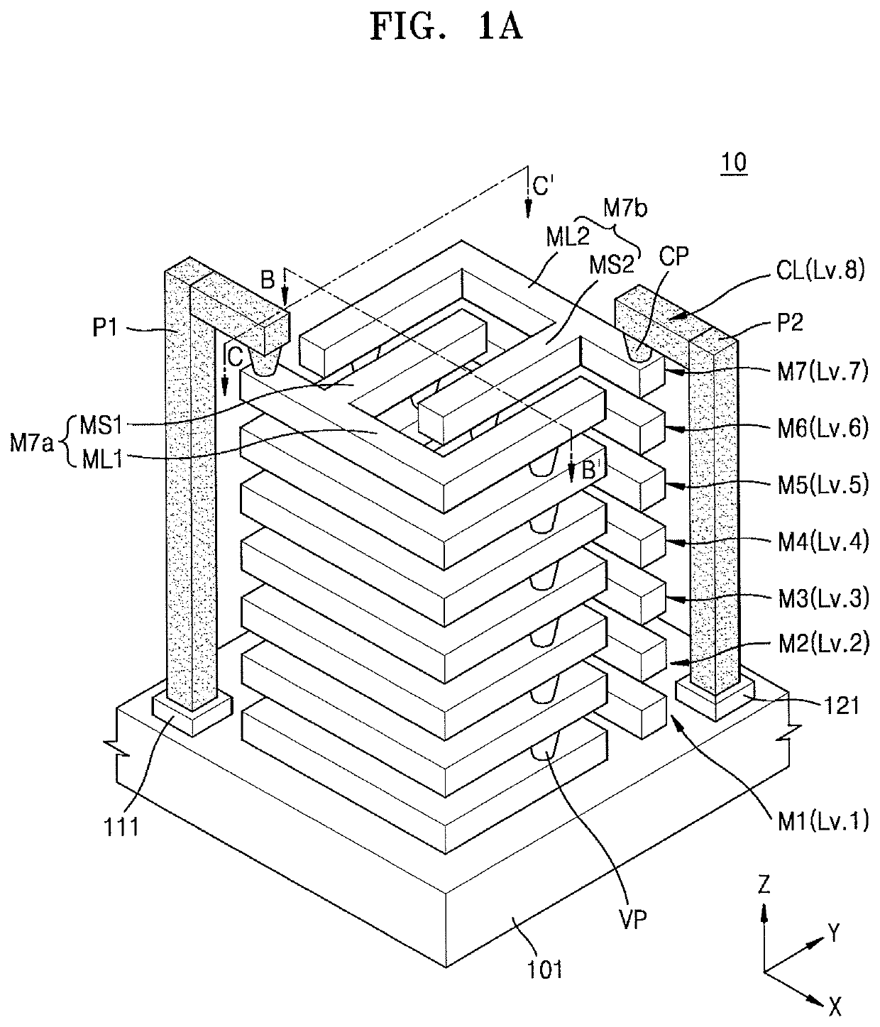
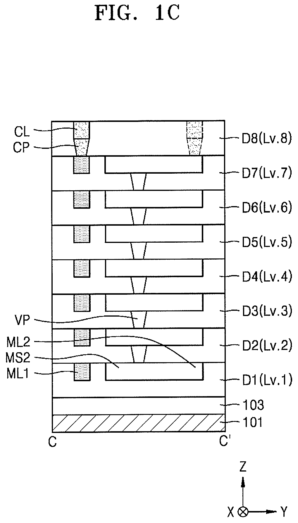
[0022]Hereinafter, embodiments will be described in detail with reference to the accompanying drawings. As used herein, the term “level” refers to a height along a vertical direction (Z direction) from a substrate. In addition, an N-th level (where N is a natural number) is closer to the substrate than an N+1-th level.

[0023]FIG. 1A is a schematic perspective view illustrating a capacitor structure according to an embodiment, and FIGS. 1B and 1C are cross-sectional views taken along lines B-B′ and C-C′ of FIG. 1A, respectively.

[0024]Referring to FIG. 1A, a capacitor structure 10 may include an electrode pad 111, a ground pad 121, a plurality of conductive pattern layers M1 to M7 respectively located at different levels Lv.1 to Lv.7, a via plug VP connecting the plurality of conductive pattern layers M1 to M7 to each other, a contact layer CL located at a higher level Lv.8 than the plurality of conductive pattern layers M1 to M7, a contact plug CP connecting the plurality of conductiv...


PUM


Abstract

A capacitor structure includes a substrate including an electrode pad and a ground pad, a plurality of dielectric layers on the substrate, the plurality of dielectric layers being at different levels on the substrate, a plurality of conductive pattern layers in at least two dielectric layers of the plurality of dielectric layers, the at least two dielectric layers of the plurality of dielectric layers being first dielectric layers, a plurality of via plugs connecting the plurality of conductive pattern layers to each other, and at least one contact layer in at least one second dielectric layer of the plurality of dielectric layers, the at least one second dielectric layer being different from the at least two first dielectric layers, and the at least one contact layer electrically connecting the plurality of conductive pattern layers to the electrode pad and the ground pad.

Description

CROSS-REFERENCE TO RELATED APPLICATION[0001]Korean Patent Application No. 10-2017-0102570, filed on Aug. 11, 2017, in the Korean Intellectual Property Office, and entitled: “Capacitor Structure and Semiconductor Device Including the Same,” is incorporated by reference herein in its entirety.BACKGROUND1. Field[0002]Embodiments relate to a capacitor structure and a semiconductor device including the same, and more particularly, to a vertical natural capacitor (VNCAP) structure and a semiconductor device including the same.2. Description of the Related Art[0003]Capacitors function to store charges and to supply charges required for operations of semiconductor devices. As semiconductor devices are highly integrated, the size of a unit cell decreases, and the capacitance required for operations of semiconductor devices increases. However, since there is a limit in selecting a dielectric material constituting a capacitor, there is a difficulty in increasing capacitance per unit area of a ...

Claims


Application Information

Patent Timeline
Patent Type & Authority Patents(United States)
IPC IPC(8): H01L29/00H01L23/522H01L49/02H01L23/528H10N99/00H10N97/00
CPCH01L28/91H01L23/5286H01L28/88H01L23/5223H01L28/40H01L28/56H01L28/75H01L21/76897H01L21/76838
Inventor KIM, JAE-WOOKIM, CHUL-KIKIM, CHUL-WANPARK, YU-KYUNGCHOI, GIL-HEYUN
Owner SAMSUNG ELECTRONICS CO LTD
Features
  • R&D
  • Intellectual Property
  • Life Sciences
  • Materials
  • Tech Scout
  • Unparalleled Data Quality
  • Higher Quality Content
  • 60% Fewer Hallucinations
Learn More