Supercharge Your Innovation With Domain-Expert AI Agents!

Optical waveguide element

a technology of optical waveguides and elements, applied in the direction of optical waveguide light guides, optical light guides, instruments, etc., can solve the problems of deterioration of optical properties, part of unnecessary light not meeting all reflection conditions, and degrading optical properties

Active Publication Date: 2020-03-17
SUMITOMO OSAKA CEMENT CO LTD
View PDF9 Cites 1 Cited by
  • Summary
  • Abstract
  • Description
  • Claims
  • Application Information

AI Technical Summary

Benefits of technology

This configuration effectively prevents refraction and leakage of unnecessary light, enhancing optical properties and allowing for a more compact design by maintaining a constant width for the waveguide collecting unnecessary light, thus improving the degree of integration and size reduction.

Problems solved by technology

According to such an optical waveguide element using the substrate, unnecessary light released from a part of an optical waveguide is coupled to other parts of the optical waveguide, and this may degrade optical properties in a case in which a plurality of optical waveguides are formed in the same substrate or in a case in which multiple branching sections and merging sections are formed in the optical waveguide in the same substrate.
Also, this may lead to deterioration of optical properties such as an ON / OFF extinction ratio in a Mach-Zehnder-type optical modulator.
As a result, a part of the unnecessary light does not satisfy all reflection conditions at a boundary of the waveguide for collecting unnecessary light on a side opposite to the side on which the waveguide for unnecessary light is connected.
Thus, there is a case in which a part of the unnecessary light is not trapped in the waveguide for collecting unnecessary light and leaks through the substrate as illustrated in FIG. 5(a), and this may degrade optical properties of the optical waveguide element.
However, according to the method, the width of the waveguide for collecting unnecessary light gradually increases with the connection of a plurality of waveguides for unnecessary light to the waveguide for collecting unnecessary light.

Method used


Image

  • Optical waveguide element
  • Optical waveguide element
  • Optical waveguide element

Examples


Embodiment Construction

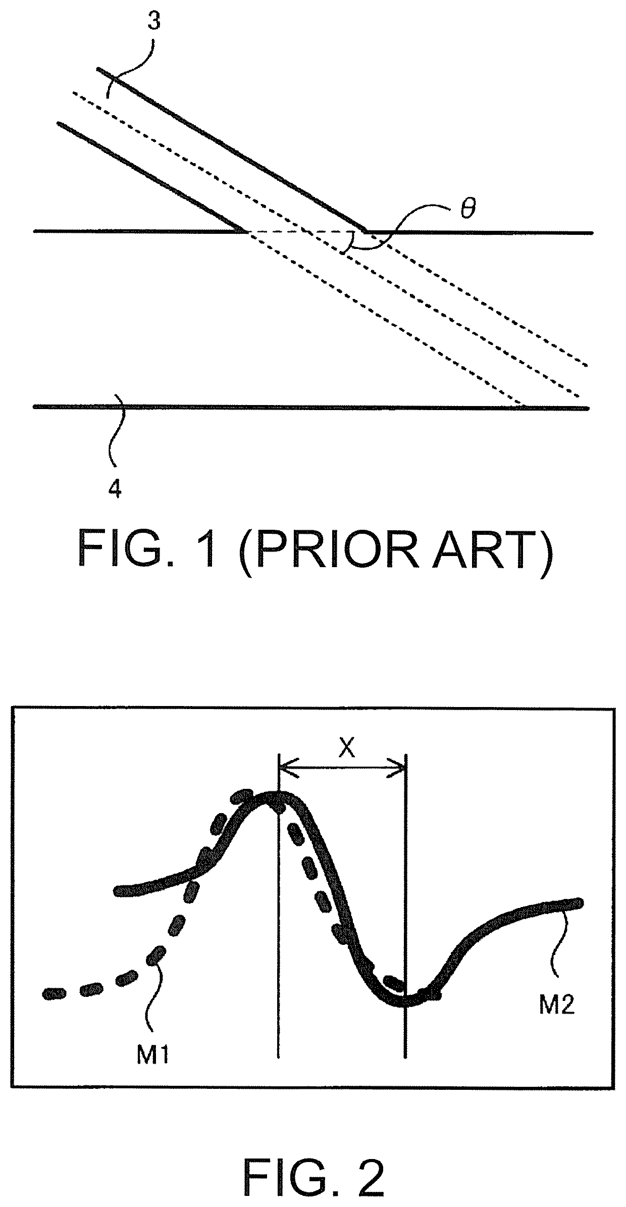
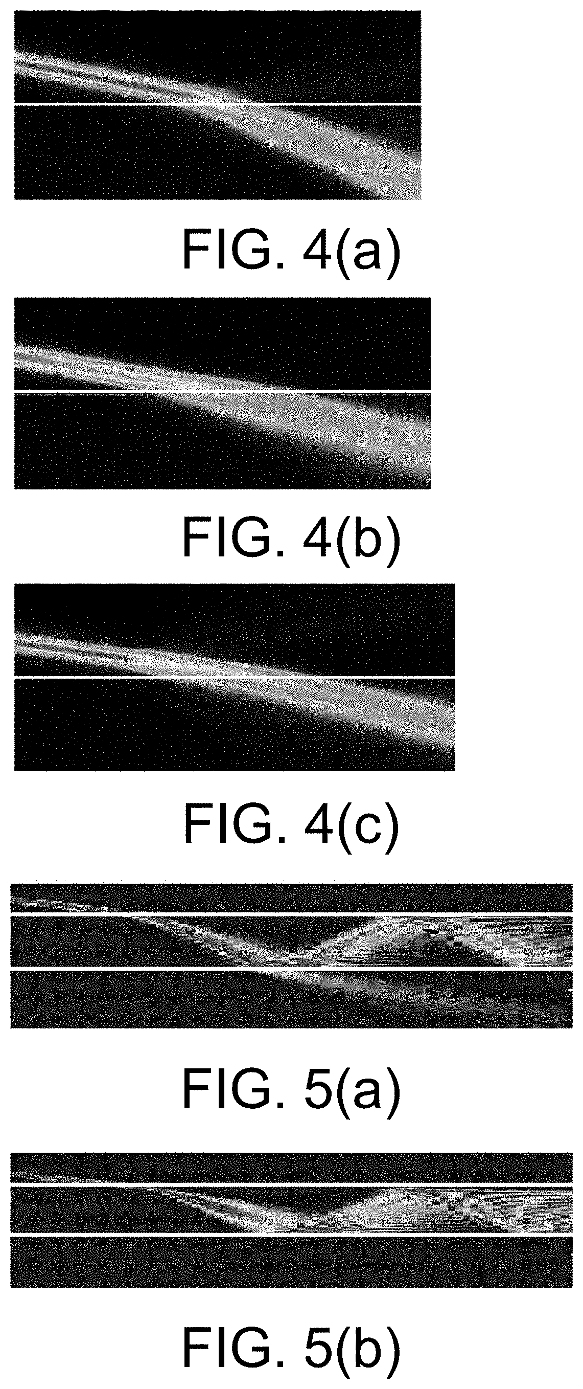
[0020]An optical waveguide element according to the disclosure will be described in detail with reference to the examples. Note that the disclosure is not limited by the examples described below. An optical waveguide element according to the disclosure is characterized in that an optical waveguide is formed on a substrate 1, the optical waveguide has a main waveguide 2 that propagates signal light, a waveguide for unnecessary light 3 that guides unnecessary light released from the main waveguide, and a waveguide for collecting unnecessary light 4 to which the unnecessary light emitted from the waveguide for unnecessary light is introduced, the waveguide for unnecessary light is connected to the waveguide for collecting unnecessary light via a waveguide for connection 5, and a width W4 of the waveguide for connection, which is a width in a direction that perpendicularly intersects a propagation direction of the unnecessary light, at a portion connected to the waveguide for collecting...


PUM

PropertyMeasurementUnit
thicknessaaaaaaaaaa
widthaaaaaaaaaa
distanceaaaaaaaaaa

Abstract

In an optical waveguide element, an optical waveguide is formed on a substrate, the optical waveguide has a main waveguide that propagates signal light, a waveguide for unnecessary light that guides unnecessary light released from the main waveguide, and a waveguide for collecting unnecessary light to which the unnecessary light emitted from the waveguide for unnecessary light is introduced, the waveguide for unnecessary light is connected to the waveguide for collecting unnecessary light via a waveguide for connection, and a width of the waveguide for connection, which is a width in a direction that perpendicularly intersects a propagation direction of the unnecessary light, at a portion connected to the waveguide for collecting unnecessary light is set to be wider than a width at a portion connected to the waveguide for unnecessary light with the waveguide for connection.

Description

CROSS-REFERENCE TO RELATED APPLICATION[0001]This application claims the priority benefit of Japan application no. 2018-055613, filed on Mar. 23, 2018. The entirety of each of the above-mentioned patent applications is hereby incorporated by reference herein and made a part of this specification.BACKGROUNDTechnical Field[0002]The present disclosure relates to an optical waveguide element with an optical waveguide formed on a substrate.Description of Related Art[0003]Optical waveguide elements provided with optical functions, such as optical modulators, have been used in many cases in the field of optical communication and the field of optical measurement. Some optical waveguide elements include optical waveguides which have higher refractive indexes than those of substrate materials due to different materials being added to substrate made of quartz, lithium niobate, semiconductors, polymer materials, or the like, or are formed as ridge-shaped protrusions on the substrate.[0004]Accord...

Claims


Application Information

Patent Timeline
Patent Type & Authority Patents(United States)
IPC IPC(8): G02B6/122G02F1/01G02B6/293G02B6/12G02F1/21
CPCG02B6/122G02B6/29352G02F1/011G02B2006/12083G02B2006/1204G02F2001/212G02B6/125G02B2006/12142G02B6/1228G02B2006/12147G02B2006/12154G02F1/212
Inventor KATAOKA, YUMIYAZAKI, NORIKAZU
Owner SUMITOMO OSAKA CEMENT CO LTD
Features
  • R&D
  • Intellectual Property
  • Life Sciences
  • Materials
  • Tech Scout
  • Unparalleled Data Quality
  • Higher Quality Content
  • 60% Fewer Hallucinations
Learn More