Supercharge Your Innovation With Domain-Expert AI Agents!

MEMS element, sealing structure, electronic device, electronic apparatus, and vehicle

a sealing structure and electronic technology, applied in fluid speed measurement, instruments, coatings, etc., can solve the problems of high manufacturing cost, high processing method, high technical difficulty, etc., and achieve excellent vehicle reliability

Active Publication Date: 2020-05-26
SEIKO EPSON CORP
View PDF37 Cites 0 Cited by
  • Summary
  • Abstract
  • Description
  • Claims
  • Application Information

AI Technical Summary

Benefits of technology

This design enables reliable and cost-effective sealing of MEMS elements, reducing manufacturing complexity and improving mechanical strength while maintaining high sealing reliability and stability.

Problems solved by technology

However, in the MEMS vibrator described in JP-A-2016-171393, in order to vacuum-seal the actuating space, there is a problem that a high-level processing method for processing the bonding surface of the lid substrate provided with a through-hole electrode into a uniform surface without irregularities is required.
Also, there is a problem that technical difficulty is high, the apparatus becomes large, and the manufacturing cost increases in order to seal the element substrate and the lid substrate together in a vacuum atmosphere (reduced pressure atmosphere).
Further, in the sealing structure in which the through-hole provided in the lid is filled with the sealing film, as described in JP-A-2007-210083, since the sealing film is disposed on the entire through-hole, there is a concern that stress relief due to a difference in the linear expansion coefficient between the lid and the sealing film cannot be sufficiently achieved and reliability of sealing may be impaired.
In the dimension of the first opening width, the dimension for which the first sealing hole can be processed is 0.1 μm or more, and when the dimension of the first opening width exceeds 2 μm, there is a concern that sealing reliability of the sealing film may be deteriorated.

Method used


Image

  • MEMS element, sealing structure, electronic device, electronic apparatus, and vehicle
  • MEMS element, sealing structure, electronic device, electronic apparatus, and vehicle
  • MEMS element, sealing structure, electronic device, electronic apparatus, and vehicle

Examples


first embodiment

MEMS Element

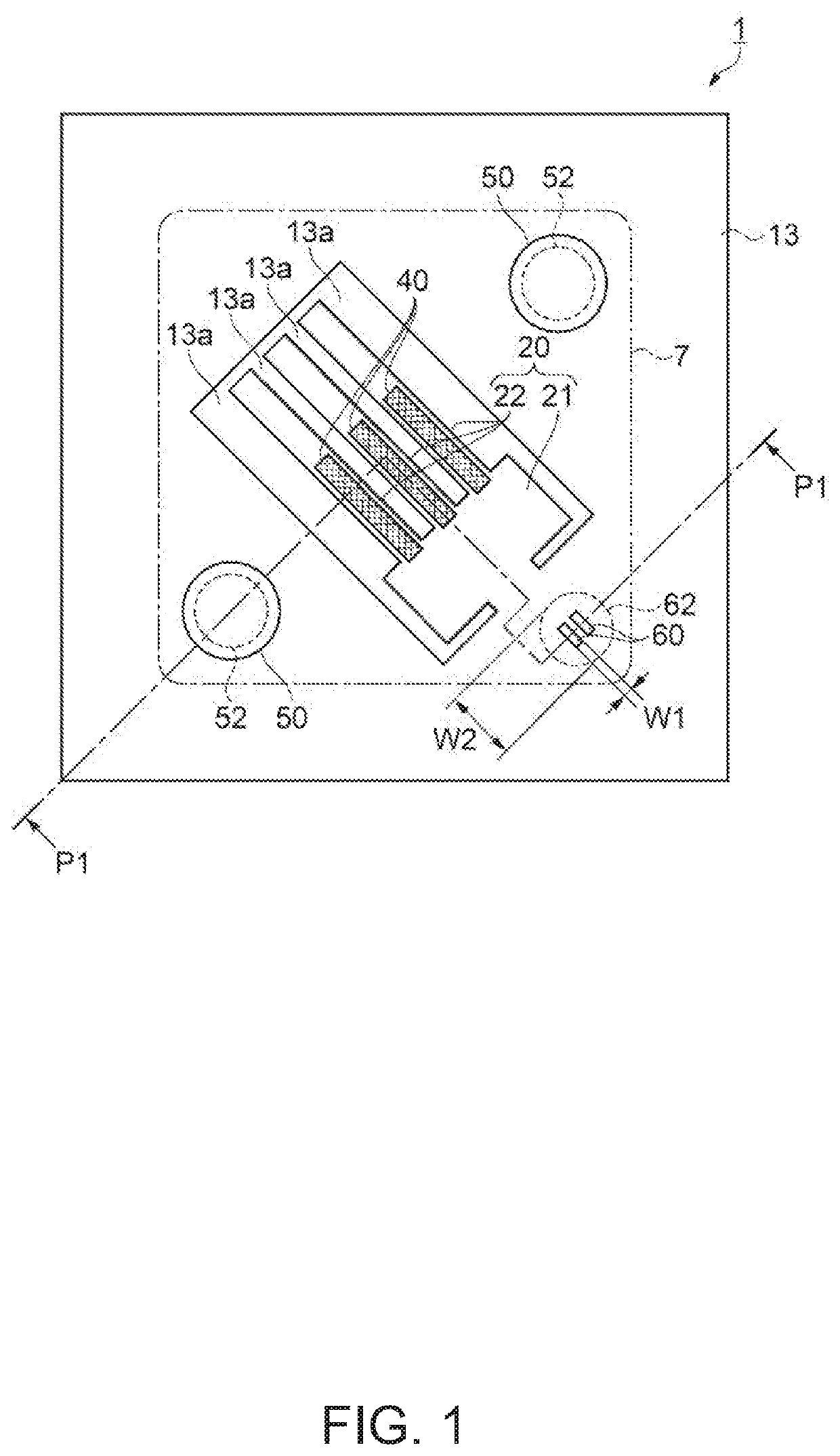
[0120]First, a MEMS element 1 according to a first embodiment will be described with reference to FIG. 1, FIG. 2A, FIG. 2B, and FIG. 2C.

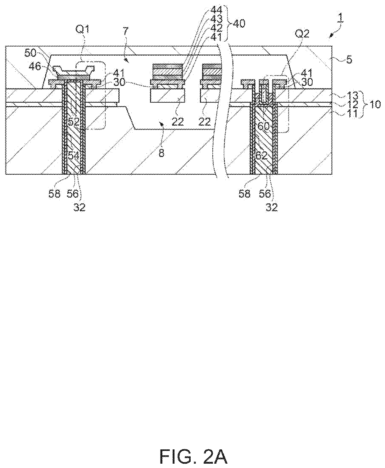
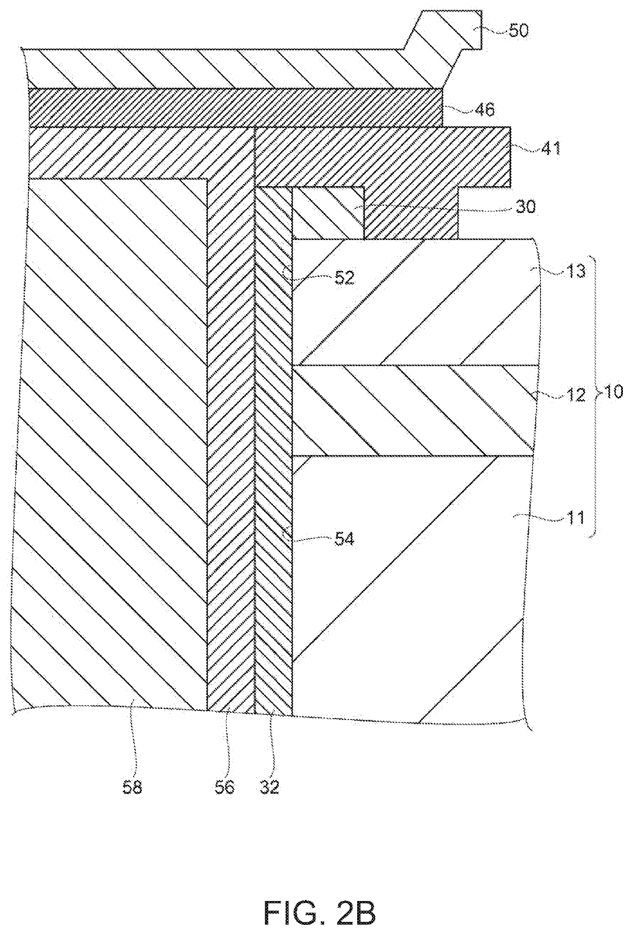
[0121]FIG. 1 is a schematic plan view illustrating a configuration of the MEMS element 1 according to the first embodiment, FIG. 2A is a schematic sectional view taken along line P1-P1 illustrated in FIG. 1, FIG. 2B is an enlarged view illustrating a Q1 portion in FIG. 2A, and FIG. 2C is an enlarged view illustrating a Q2 portion in FIG. 2A. In FIG. 1, for convenience of explanation of an internal structure of the MEMS element 1, a state in which a lid 5 is removed is illustrated. In FIGS. 2A, 2B and 2C, a line illustrating a background of a cross-section is omitted.

[0122]As illustrated in FIGS. 1, 2A, 2B, and 2C, the MEMS element 1 according to the present embodiment is configured to include the lid 5 for airtightly sealing an element 20 and a silicon on insulator (SOI) substrate 10 on which the element 20 is formed. In the present embo...

second embodiment

MEMS Element

[0176]Next, a MEMS element 1a according to a second embodiment will be described with reference to FIG. 4.

[0177]FIG. 4 is a schematic cross-sectional view corresponding to a position of the line P1-P1 of FIG. 1 illustrating a configuration of a MEMS element 1a according to the second embodiment. Description will be mainly made on differences from the embodiment described above, and the same reference numerals are given to similar configurations, and description of similar matters will be omitted.

[0178]The MEMS element 1a according to the second embodiment differs from the MEMS element 1 according to the first embodiment in structures of a second wiring through-hole 54a and a second sealing hole 62a.

[0179]As illustrated in FIG. 4, in the MEMS element 1a of the present embodiment, the second wiring through-hole 54a and the second sealing hole 62a disposed in the silicon layer 11 and the BOX layer 12 have a tapered portion that expands toward a surface of the support subst...

third embodiment

MEMS Element

[0181]Next, a MEMS element 1b according to a third embodiment will be described with reference to FIG. 5.

[0182]FIG. 5 is an enlarged view of a schematic cross-section corresponding to a position of the Q2 portion in FIG. 2A illustrating a configuration of the MEMS element 1b according to the third embodiment. Description will be mainly made on differences from the embodiments described above, and the same reference numerals are given to similar configurations, and description of similar matters will be omitted.

[0183]The MEMS element 1b according to the third embodiment is different from the MEMS element 1 according to the first embodiment in a structure of a wiring electrode 56b which becomes the sealing film of the first sealing hole 60.

[0184]As illustrated in FIG. 5, in the MEMS element 1b of the present embodiment, the wiring electrode 56b is composed of two layers of a first layer 71 and a second layer 72, and the first layer 71 is disposed closer to the inner space ...


PUM

PropertyMeasurementUnit
thicknessaaaaaaaaaa
thicknessaaaaaaaaaa
aspect ratioaaaaaaaaaa

Abstract

A MEMS element includes a surface silicon layer on which an element is formed and on which a first electrode and a second electrode as element electrodes and an electrode pad connected to the first electrode and the second electrode are disposed, and in which a first wiring through-hole is disposed at a position overlapping with the electrode pad of the surface silicon layer and a wiring electrode electrically connected to the electrode pad is disposed in the first wiring through-hole, in plan view.

Description

CROSS-REFERENCE TO RELATED APPLICATIONS[0001]This application claims priority to Japanese Patent Application No. 2017-087982, filed Apr. 27, 2017, No. 2017-146224, filed Jul. 28, 2017, No. 2017-097934, filed May 17, 2017, No. 2017-106272, filed May 30, 2017, No. 2017-087986, filed Apr. 27, 2017, and No. 2017-146226, filed Jul. 28, 2017, the entirety of which are hereby incorporated by reference.BACKGROUND1. Technical Field[0002]The present invention relates to a MEMS element, a sealing structure, an electronic device, an electronic apparatus, and a vehicle.2. Related Art[0003]In the related art, a MEMS vibrator in which an actuating element is formed on a silicon substrate using a micro electro mechanical system (MEMS) technology is known. For example, in the following JP-A-2016-171393, a method of manufacturing a MEMS vibrator by bonding a lid substrate also formed of a silicon substrate and provided with a through-hole electrode (TSV: Through Silicon Via) for external connection t...

Claims


Application Information

Patent Timeline
Patent Type & Authority Patents(United States)
IPC IPC(8): B81B7/00B81C1/00
CPCB81B7/007B81C1/00301B81B2207/096
Inventor YAMAZAKI, TAKASHIEBINA, AKIHIKOKAWAUCHI, OSAMUYOKOYAMA, YOSHIHIKO
Owner SEIKO EPSON CORP
Features
  • R&D
  • Intellectual Property
  • Life Sciences
  • Materials
  • Tech Scout
  • Unparalleled Data Quality
  • Higher Quality Content
  • 60% Fewer Hallucinations
Learn More