Display panel and method for fabricating display panel
a display panel and display panel technology, applied in the field of display panels, can solve the problems of large processing volume, waste of raw materials, high cost, etc., and achieve the effects of saving process quantity and process complexity, and reducing raw material cost and production cos
- Summary
- Abstract
- Description
- Claims
- Application Information
AI Technical Summary
Benefits of technology
Problems solved by technology
Method used
Image

Examples
first embodiment
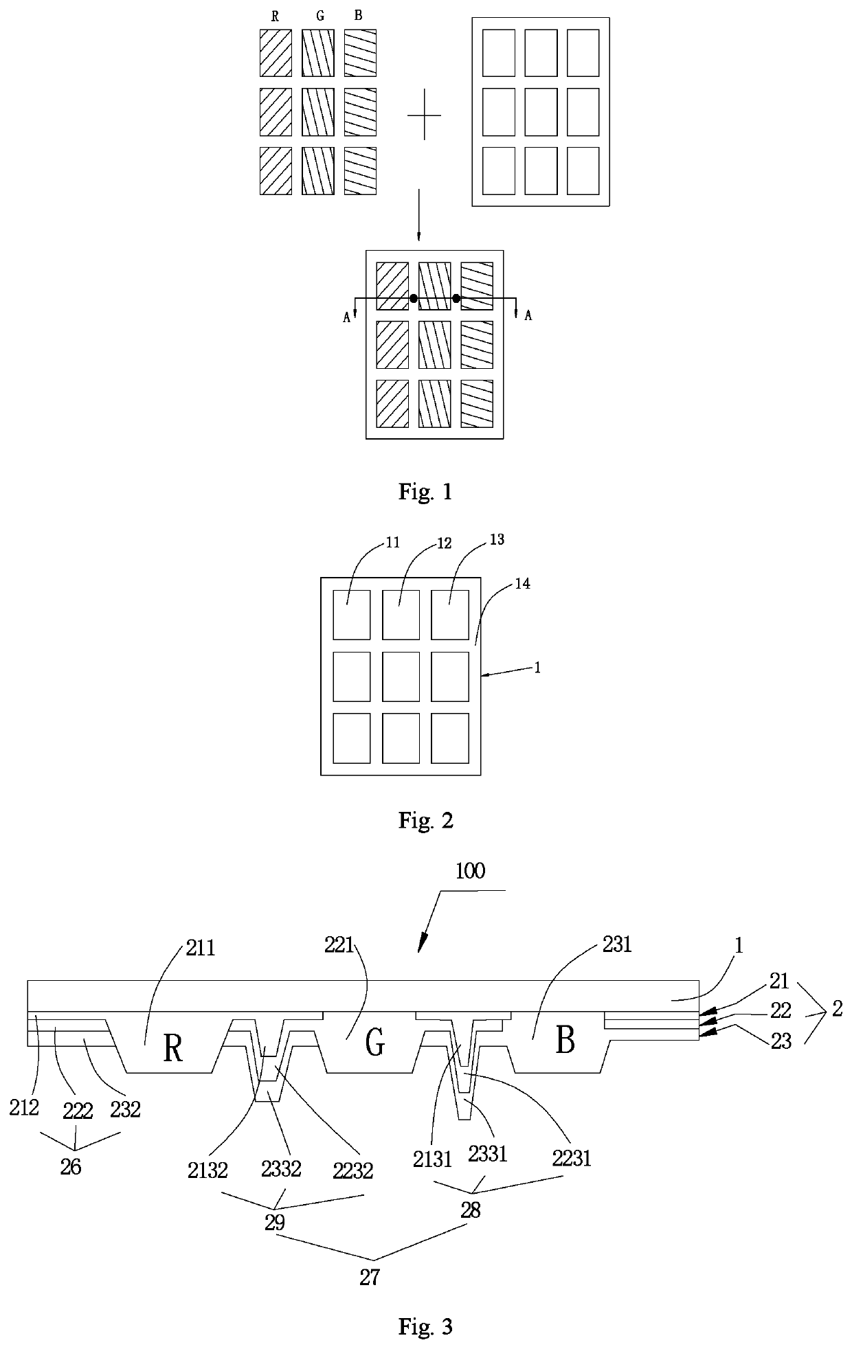
[0041]Please refer to FIGS. 1-4, in the color filter substrate 100 of the display panel provided by the present application, the first color resistance block 211, the second color resistance block 221 and the third color resistance block 231 are all island-shaped. The first color resistance block 211 is disposed corresponding to the first color resistance region 11 of the substrate base layer 1, the second color resistance block 221 is disposed corresponding to the second color resistance region 12, and the third color resistance block 231 is disposed corresponding to the third color resistance region 13. The first color resistance block 211, the second color resistance block 221, and the third color resistance block 231 respectively correspond to the open regions of the red, green, and blue sub-pixels, acting as red, green, and blue filters respectively.
[0042]In the fourth region 14 of the substrate base layer 1, the first color resistance film 212, the second color resistance film...
second embodiment
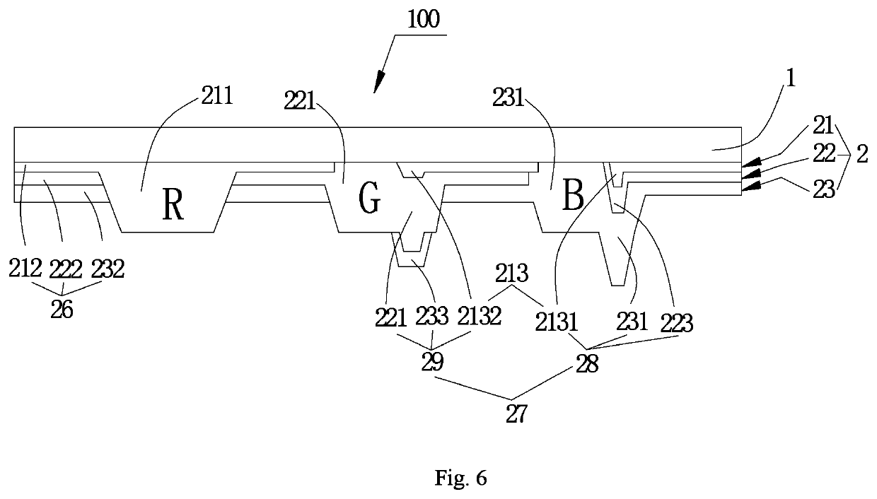
[0051]Please refer to FIGS. 5-6, in the color filter substrate 100 of the display panel provided by the present application, the first color resistance block 211, the second color resistance block 221 and the third color resistance block 231 are strip-shaped. The first color resistance block 211 is disposed in accordance with the plurality of the first color resistance regions 11 and a portion of the fourth region 14 between adjacent two of the first color resistance regions 11, the second color resistance block 221 is disposed in accordance with the plurality of the second color resistance regions 12 and a portion of the fourth region 14 between adjacent two of the second color resistance regions 12, and the third color resistance block 231 is disposed in accordance with the plurality of the third color resistance regions 13 and a portion of the fourth region 14 between adjacent two of the third color resistance regions 13.
[0052]The portion of the first color resistance block 211 c...
third embodiment
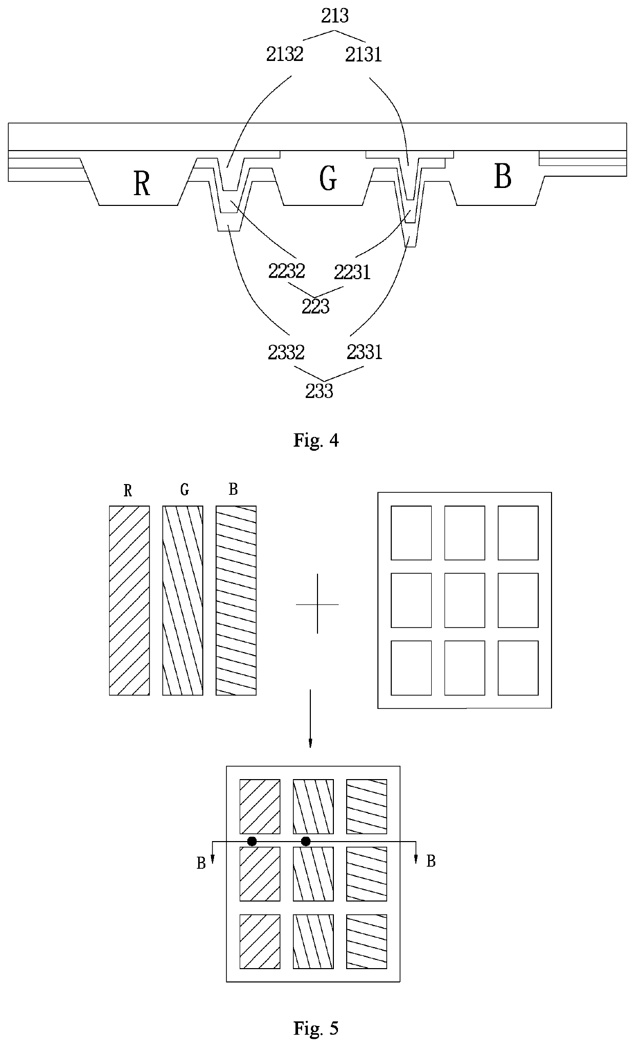
[0069]Specifically, please refer to the third embodiment as shown in FIGS. 8-10.
[0070]In the step S2 as shown in FIG. 8, the first color resistance block 211 is island-shaped, and is arranged in accordance with the first color resistance region 11. In the fourth region 14 of the substrate base layer 1, the first color resistance film 212 and the second color resistance pillar 223 are formed, wherein the first color resistance pillar 213 is divided into a first primary color resistance pillar portion 2131 and a first secondary color resistance pillar portion 2132. The height R21 of the first primary color resistance pillar portion 2131 is greater than the height R22 of the first secondary resistance pillar portion 2132, and the first primary color resistance pillar portion 2131 and the first secondary color resistance pillar portion 2132 are spaced from each other. For example, in the third embodiment, the first primary color resistance pillar portion 2131 is disposed between the sec...
PUM
| Property | Measurement | Unit |
|---|---|---|
| height | aaaaa | aaaaa |
| height | aaaaa | aaaaa |
| height | aaaaa | aaaaa |
Abstract
Description
Claims
Application Information
 - R&D
- Intellectual Property
- Life Sciences
- Materials
- Tech Scout
- Unparalleled Data Quality
- Higher Quality Content
- 60% Fewer Hallucinations
Browse by: Latest US Patents, China's latest patents, Technical Efficacy Thesaurus, Application Domain, Technology Topic, Popular Technical Reports.
© 2025 PatSnap. All rights reserved.Legal|Privacy policy|Modern Slavery Act Transparency Statement|Sitemap|About US| Contact US: help@patsnap.com