Electroluminescent display device
a technology of electroluminescent display device and display device, which is applied in the direction of solid-state devices, semiconductor devices, organic semiconductor devices, etc., can solve the problems of degrading the light extraction efficiency of the electroluminescent display device b>1/b>, and achieve the effect of improving light extraction efficiency and reliability
- Summary
- Abstract
- Description
- Claims
- Application Information
AI Technical Summary
Benefits of technology
Problems solved by technology
Method used
Image

Examples
first embodiment
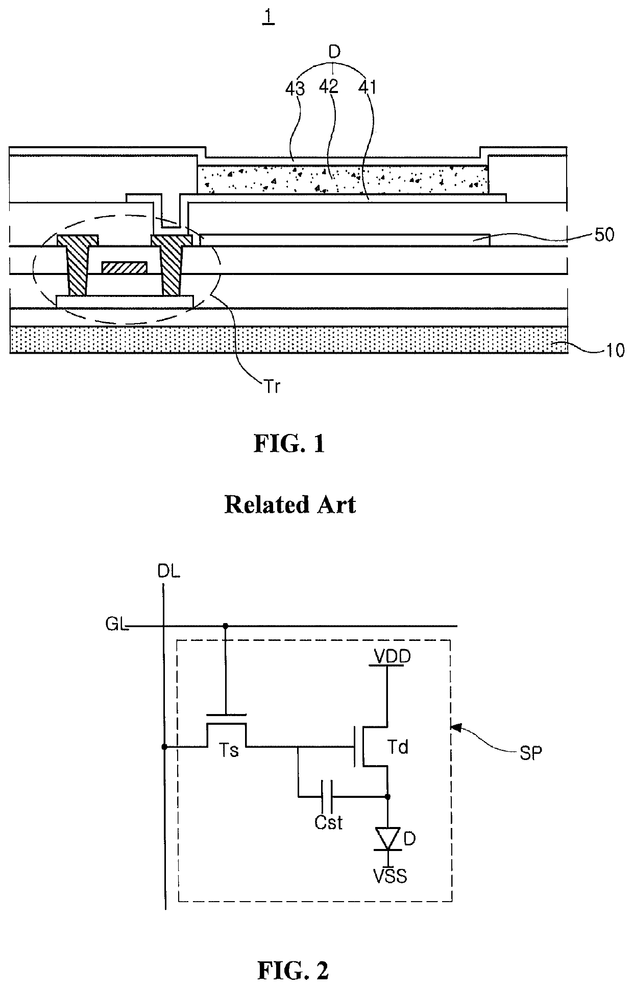
[0029]FIG. 2 is a circuit diagram illustrating a subpixel area of an electroluminescent display device according to an embodiment of the present disclosure.
[0030]As illustrated in FIG. 2, the electroluminescent display device according to the embodiment of the present disclosure includes a gate line GL, a data line DL, a switching thin film transistor Ts, a driving thin film transistor Td, a storage capacitor Cst and a light-emitting diode D. The gate line GL and the data line DL cross each other to define a subpixel area SP. The switching thin film transistor Ts, the driving thin film transistor Td, the storage capacitor Cst and the light-emitting diode D are formed in the subpixel area SP.
[0031]More specifically, a gate electrode of the switching thin film transistor Ts is connected to the gate line GL and a source electrode of the switching thin film transistor Ts is connected to the data line DL. A gate electrode of the driving thin film transistor Td is connected to a drain ele...
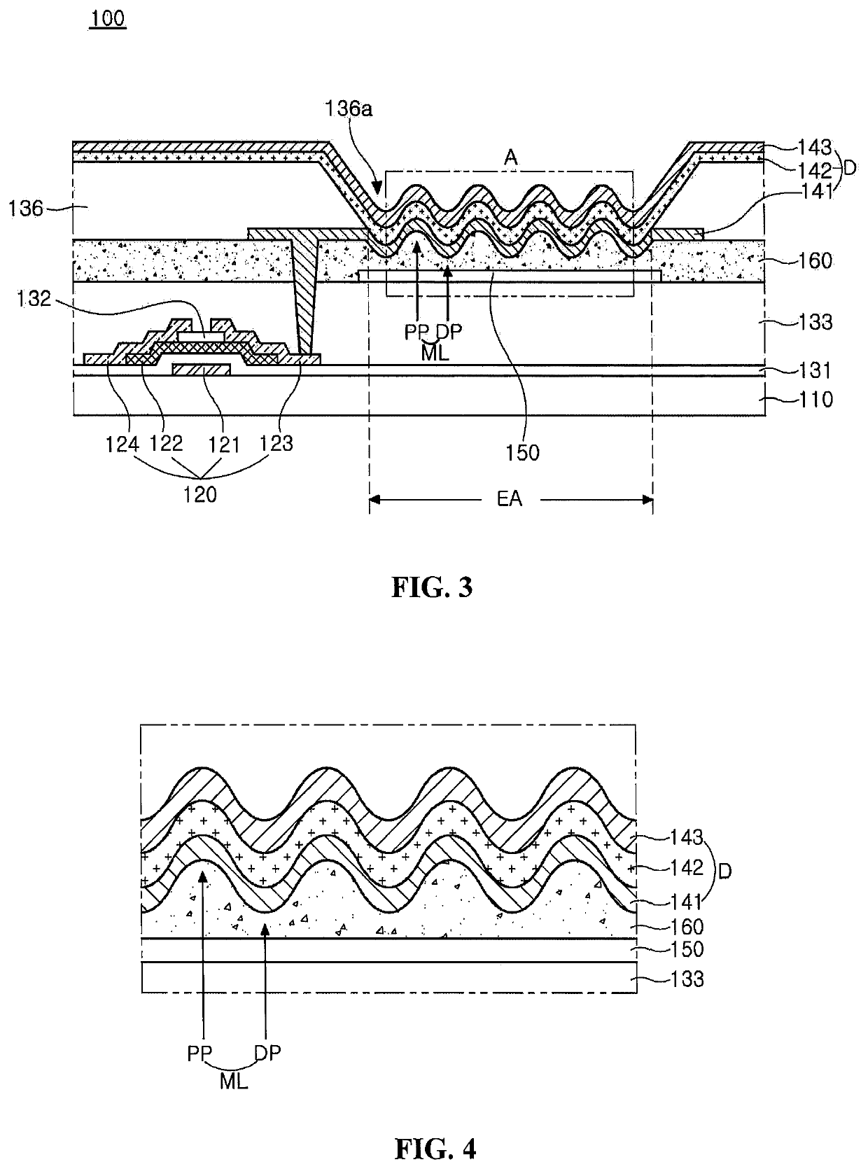
second embodiment
[0115]Hereinafter, detailed description of configurations identical or similar to those of the first embodiment may be omitted.
[0116]FIG. 7 is a cross-sectional view schematically illustrating an electroluminescent display device according to a second embodiment of the present disclosure.
[0117]As illustrated in FIG. 7, an electroluminescent display device 200 according to a second embodiment of the present disclosure includes a substrate 210, a thin film transistor 220, a color filter pattern 250, an overcoat layer 260, and a light-emitting diode D electrically connected to the thin film transistor 220.
[0118]The thin film transistor 220 may include a gate electrode 221, an active layer 222, a source electrode 223, and a drain electrode 224.
[0119]Specifically, the gate electrode 221 of the thin film transistor 220 and a gate insulating layer 231 may be disposed on the substrate 210.
[0120]The active layer 222 which overlaps the gate electrode 221 may be disposed on the gate insulating...
PUM
| Property | Measurement | Unit |
|---|---|---|
| voltage | aaaaa | aaaaa |
| driving voltage | aaaaa | aaaaa |
| driving voltage | aaaaa | aaaaa |
Abstract
Description
Claims
Application Information
 - R&D
- Intellectual Property
- Life Sciences
- Materials
- Tech Scout
- Unparalleled Data Quality
- Higher Quality Content
- 60% Fewer Hallucinations
Browse by: Latest US Patents, China's latest patents, Technical Efficacy Thesaurus, Application Domain, Technology Topic, Popular Technical Reports.
© 2025 PatSnap. All rights reserved.Legal|Privacy policy|Modern Slavery Act Transparency Statement|Sitemap|About US| Contact US: help@patsnap.com