Compound for organic electronic element, organic electronic element using the same, and an electronic device thereof

Active Publication Date: 2022-05-10
DUK SAN NEOLUX
View PDF9 Cites 0 Cited by
  • Summary
  • Abstract
  • Description
  • Claims
  • Application Information

AI Technical Summary

Benefits of technology

[0014]By using the compound according to the present invention, high luminous efficiency, low driving voltage and hig

Problems solved by technology

However, when only one material is used as a light emitting material, due to intermolecular interaction, the maximum emission wavelength shifts to a longer wavelength, and there are problems in that the color purity is lowered or the device efficiency is reduced due to the emission attenuation effect, therefore in order to increase color purity and increase luminous efficiency through energy transfer, a host/dopant system may be used as a light emitting material.
Currently, the portable display market is a large-area display, and the size thereof is increasing, and thus, more power consumption than the power consumption required for the existing portable display is required.
Therefore, power consumption has become a very important factor for a portable display having a limited power supply such as a battery, and the probl

Method used


Image

  • Compound for organic electronic element, organic electronic element using the same, and an electronic device thereof
  • Compound for organic electronic element, organic electronic element using the same, and an electronic device thereof
  • Compound for organic electronic element, organic electronic element using the same, and an electronic device thereof

Examples


Example

[Example 1]: Red Organic Light Emitting Device (Phosphorescent Host)

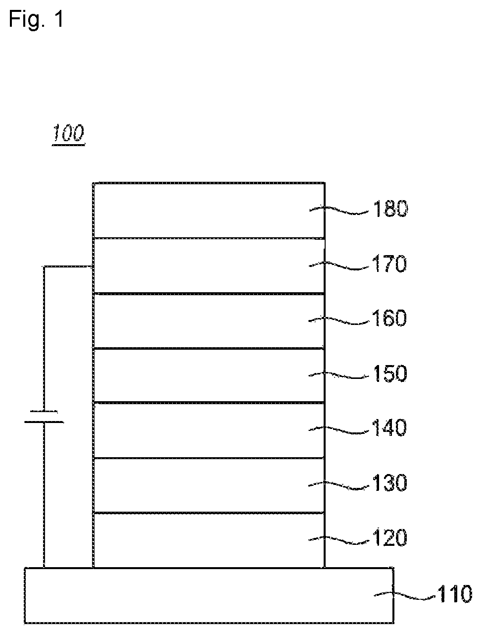
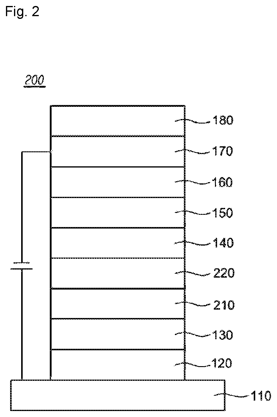
[0167]An organic electroluminescent device was manufactured according to a conventional method by using the compound obtained through synthesis as a light emitting host material of the emitting layer. First, a N1-(naphthalen-2-yl)-N4, N4-bis(4-(naphthalen-2-yl(phenyl)amino)phenyl)-N1-phenylbenzene-1,4-diamine (abbreviated as 2-TNATA) film was vacuum-deposited on the ITO layer (anode) formed on a glass substrate to form a 60 nm-thick hole injection layer, and 4,4-bis[N-(1-naphthyl)-N-phenylamino]biphenyl (hereinafter abbreviated as —NPD) as a hole transport compound on the hole injection layer was vacuum-deposited to a thickness of 60 nm to form a hole transport layer.

[0168]As a host on the hole transport layer, the compound (P-1) of the present invention represented by Formula (1) and DSNL1 were used in a weight ratio (5:5), and (piq)2Ir(acac)[bis-(1-phenylisoquinolyl)iridium(III)acetylacetonate] as a dopant materia...

Example

[Example 2] to [Example 14]

[0170]An organic electroluminescent device was prepared in the same manner as in Example 1, except that the compound DSNL1 or DSNL2 and the compound of the present invention described in Table 5 were used instead of the compound (P-1) of the present invention as the host material of the emitting layer.

Example

[Comparative Example 1] to [Comparative Example 12]

[0171]An organic electroluminescent device was prepared in the same manner as in Example 1, except that the compound DSNL1 or DSNL2 and Comparative Compound A to Comparative Compound F were used as the host material of the emitting layer.

[0172]

[0173]

[0174]By applying a forward bias DC voltage to the organic electronic devices prepared in Examples 1 to 14 and Comparative Examples 1 to 12 prepared in this way, Electroluminescence (EL) characteristics were measured with PR-650 from photo research, and as a result of the measurement, the T95 lifetime was measured using a lifetime measuring device manufactured by McScience at 2500 cd / m2 standard luminance. Table 5 below shows the device fabrication and evaluation results.

[0175]TABLE 5CurrentFirstSecondVoltageDensityBrightnessEfficiencycompoundcompound(v)(mA / cm2)(cd / m2)(cd / A)T(95)comparativeDSNL1comparative5.315.8250015.8109.8example(1)compound Acomparativecomparative5.316.0250015.6108.0e...


PUM


Abstract

Provided are a novel compound capable of improving the luminous efficiency, stability and lifespan of an element, an organic electronic element using the same, and an electronic device thereof.

Description

BACKGROUNDTechnical Field[0001]The present invention relates to a compound for an organic electronic element, an organic electronic element using the same, and an electronic device thereof.Background Art[0002]In general, organic light emitting phenomenon refers to a phenomenon that converts electric energy into light energy by using an organic material. An organic electronic element using an organic light emitting phenomenon usually has a structure including an anode, a cathode, and an organic material layer interposed therebetween. Here, in order to increase the efficiency and stability of the organic electronic element, the organic material layer is often composed of a multi-layered structure composed of different materials, and for example, may include a hole injection layer, a hole transport layer, an emitting layer, an electron transport layer, an electron injection layer and the like.[0003]A material used as an organic material layer in an organic electronic element may be cla...

Claims


Application Information

Patent Timeline
IPC IPC(8): C07D487/04H01L51/00H01L51/50
CPCH01L51/0072C07D487/04H01L51/0061H01L51/0074H01L51/5016Y02E10/549H10K85/6572H10K85/636H10K85/6576H10K50/11H10K2101/10
Inventor YOO, JAE DUKPARK, JONG GWANGMUN, SOUNG YUNLEE, YUN SUKLEE, IN GOOLI, GUANG MING
Owner DUK SAN NEOLUX
Why Eureka
Try Eureka