Woven or ink jet printed arrays for extreme UV and X-ray source and detector

Inactive Publication Date: 2002-01-24
INTELLECTUAL VENTURES FUND 83 LLC +1
View PDF0 Cites 15 Cited by
  • Summary
  • Abstract
  • Description
  • Claims
  • Application Information

AI Technical Summary

Benefits of technology

0015] Method and means are disclosed for eliminating barrier contacts required in prior art diode devices. Examples of such diode devices are presented in the cited patents and applications. The barrier contacts reduced efficiency of both photoconduction and photoemission of the prior art diode devices. Photoconduction and photoemission are increased by the use of a triode array of organic junction field effect transistor (OJFET) devices, each having a surrounding gate that controls carrier energy and balance. True ohmic contacts inject carriers and fill interface and bulk traps, thereby increasing carrier mobility of the OJFET devices by a factor approaching 10.sup.5. These true ohmic contacts also increasing space-charge distance by a factor of 50 or more.
0016] An OJFET is functionally a monocolor pixel, and is also functionally operable to sense radiation and, alternately, to emit radiation about a design of center wavelength between 150 nm and 100 nm. The pixel OJFET operates in a short-channel, normally OFF, gate-controlled mode. Pixels are also preferably operated in an array. For operation in a photoconduction and sensing mode, the devices of the array are biased near avalanche. Sensing a query, the illuminated part of the array will avalanche multiply the impinging radiation for detection and decoding. In transmitting a query or in responding to a recognized query, the array of pixels programmed with

Problems solved by technology

The barrier contacts reduced efficiency of both photocon

Method used


Image

  • Woven or ink jet printed arrays for extreme UV and X-ray source and detector
  • Woven or ink jet printed arrays for extreme UV and X-ray source and detector
  • Woven or ink jet printed arrays for extreme UV and X-ray source and detector

Examples


Embodiment Construction

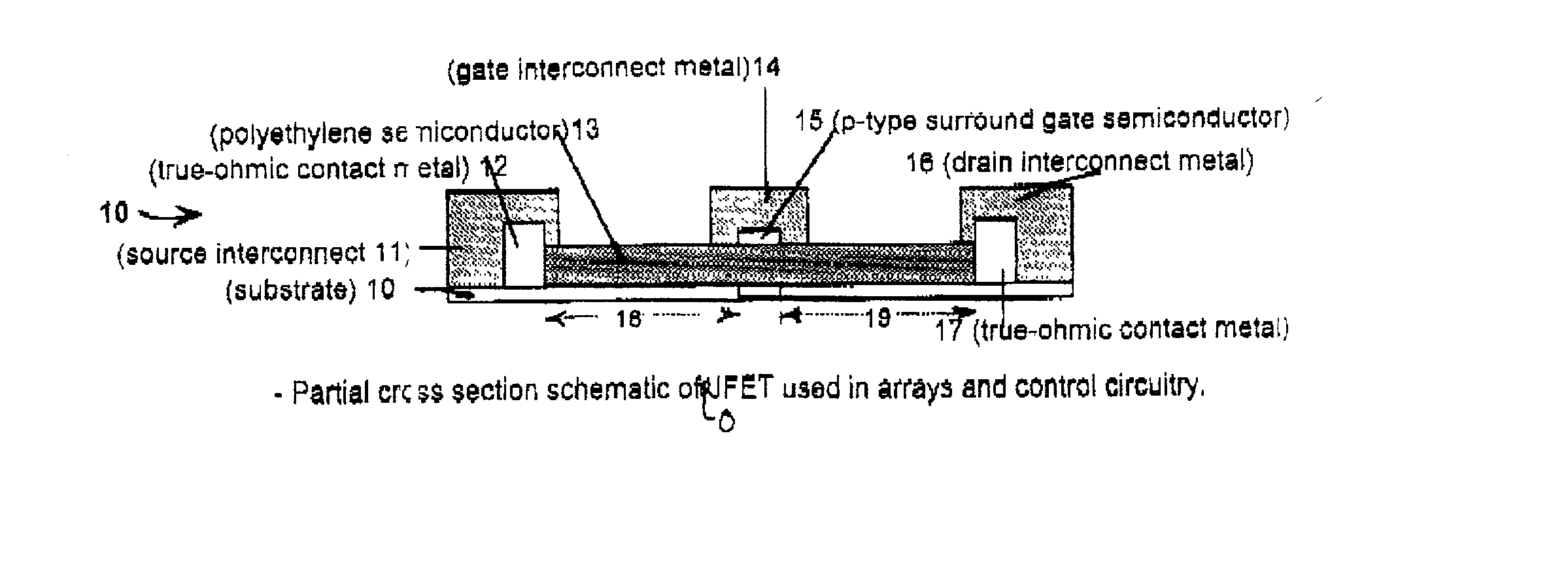
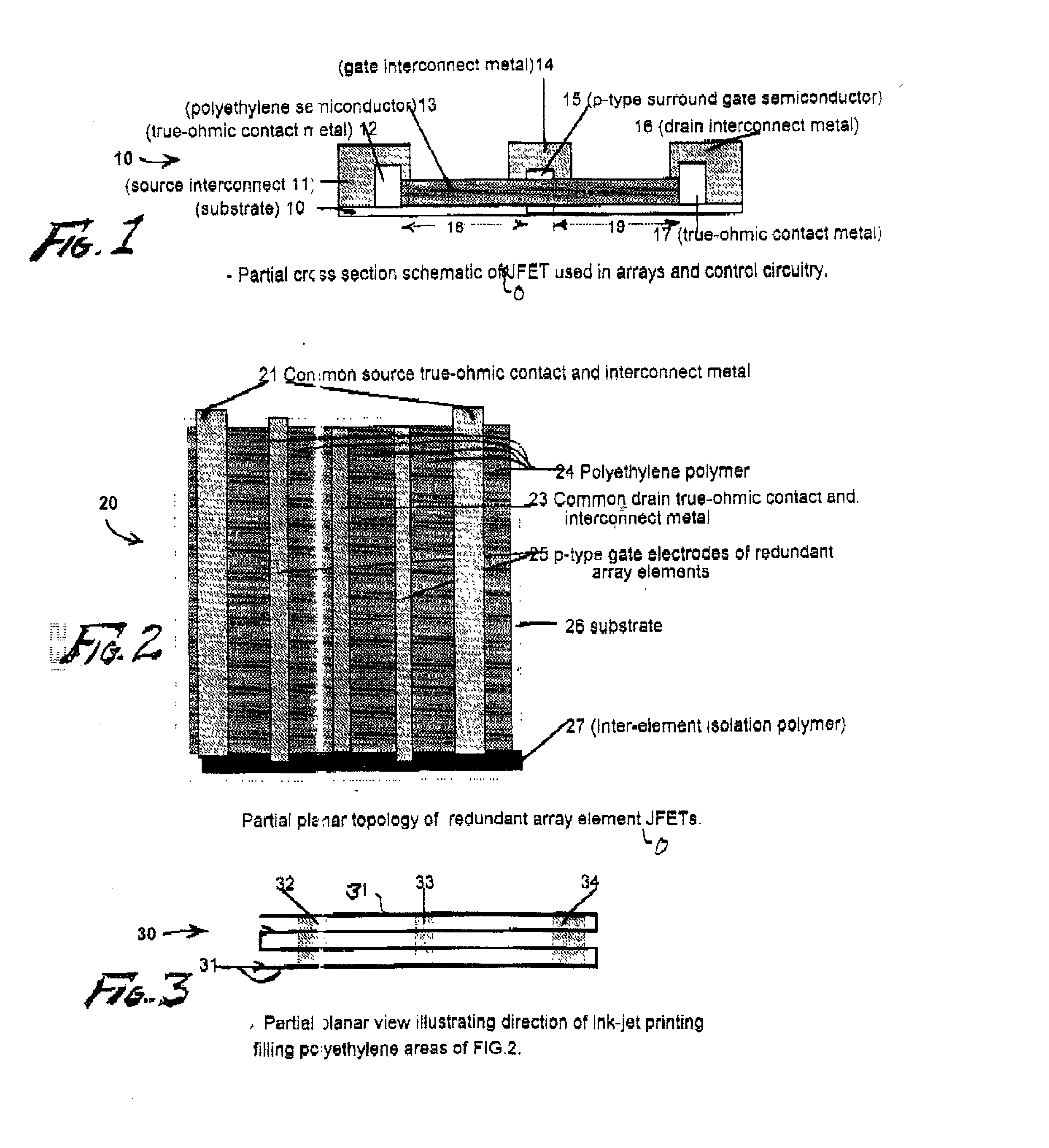
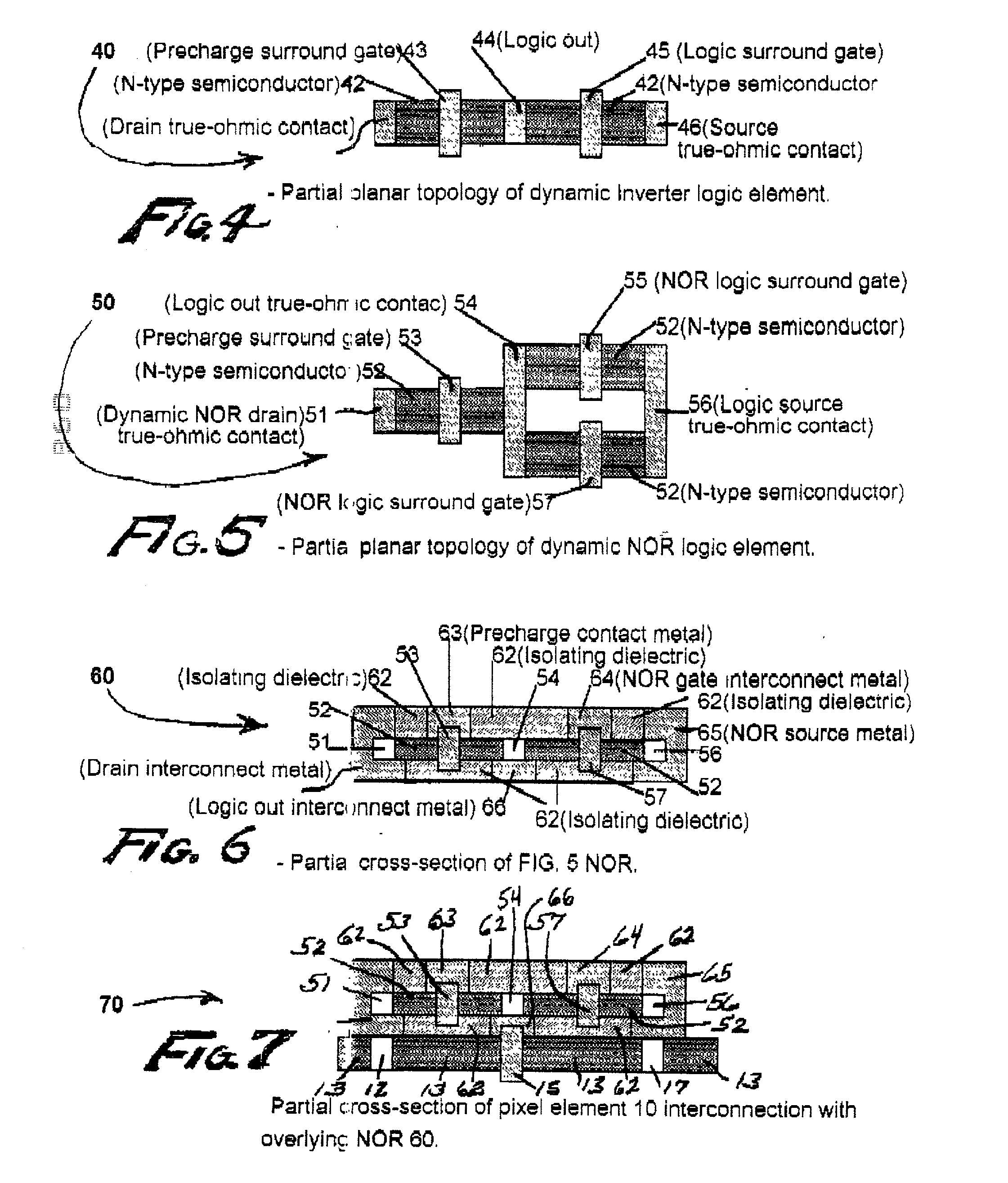
[0028] This invention comprises triode electroluminescent polymer and co-polymer devices, structures, arrays and materials which are designed to transmit and receive radiation in the extreme. The triode devices are functional to radiation at its design center wavelength between 150 nm and 100 nm. More specifically, they can function as an emitter of radiation at its design center wavelength, or conversely, as a sensor of radiation at its design center wavelength. The triode are preferably configured in arrays and combined with programmable control systems to form photoconduction and photoemission apparatus for use in (a) exposure of photoresist in integrated circuit manufacture, (b) two-way communication devices, (c) identification and detection processes and (d) medical and other products and photonic devices.

[0029] The invention utilizes prior art and referenced principles, materials and means for providing true solid / solid interface Mott-Gurney, no-barrier, true-ohmic contact to ...


PUM


Abstract

Polymer photoconduction and photoemission devices and arrays for use in photoresist, two-way communication, identification and detection processes, and other products and photonic devices. The apparatus is functionally responsive to X-ray and EUV radiation. The apparatus is preferably embodied in an array which can both sense and emit UV radiation at around wavelengths lambd=145 nm to lambd 100 nm. The devices can be fabricated by forming woven polymer fibers or ink-jet printed polymers into an array or arrays. Each array can also be integrally fabricated with address and control circuitry required to obtain the desired functionality.

Description

[0001] This disclosure is a continuation-in-part of U.S. application Ser. No. 09 / 823,269, filed Mar. 30, 2001, which is a continuation-in-part of U.S. application Ser. No. 09 / 218,233, filed Dec. 22, 1998.BACKGROUND OF THE DISCLOSURE[0002] 1. Field of the Invention[0003] This invention is directed toward polymer photoconduction and photoemission devices and arrays for use in photoresist exposure, two-way communication, identification and detection processes and other products and photonic devices. More specifically, the invention is directed toward programmable arrays which operate efficiently to produce and / or sense radiation with wavelength .lambda. at about .lambda.=150 nm to .lambda.=100 nm in the extreme ultra violet (EUV) and X-ray region. Such arrays are fabricated by forming woven polymer fibers, or alternately by ink-jet printed polymers into an array or arrays, wherein each array comprises integrally fabricated address and control circuitry.[0004] 2. Description of the Rela...

Claims


Application Information

Patent Timeline
IPC IPC(8): H01L27/32H01L29/76H01L51/10H01L51/52H05B33/14
CPCH01L27/308H01L27/32H01L27/3211H01L51/0508H01L51/0512H01L51/102H01L51/105H01L51/5203H01L51/5287H01L51/5296H10K39/36H10K59/00H10K59/35H10K10/46H10K10/462H10K10/82H10K10/84H10K50/805H10K50/182H10K50/30
Inventor CHRISTENSEN, ALTON O.
Owner INTELLECTUAL VENTURES FUND 83 LLC
Why Eureka
Try Eureka