Low triggering N MOS transistor for ESD protection working under fully silicided process without silicide blocks
a low-triggering n-mos transistor and esd protection technology, applied in the direction of transistors, semiconductor devices, semiconductor/solid-state device details, etc., can solve the problems of reducing esd performance, ldd junction silicide, and high snapback voltage of some devices
- Summary
- Abstract
- Description
- Claims
- Application Information
AI Technical Summary
Problems solved by technology
Method used
Image

Examples
first embodiment
[0042] Method for First Embodiment
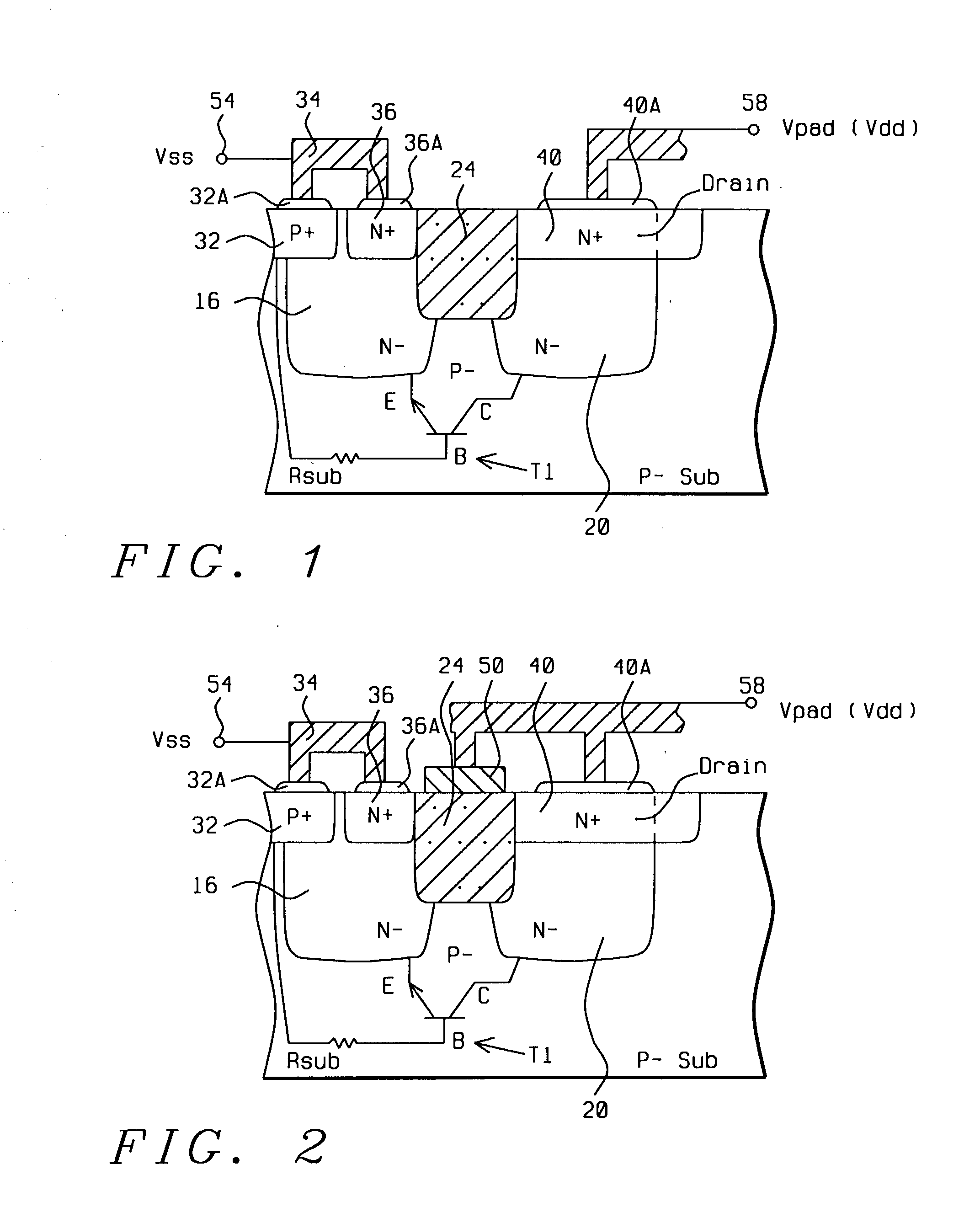
[0043] We form a first n+ region 40 and a second n+ region 36 are separated by a first isolation region 24 in a substrate 10. The substrate 10 is p- doped.
[0044] We form a first n- well 20 overlaps only a portion of the first isolation region 24 and overlapping a portion of the first n+ region 40.
[0045] We form a first p+ region 32 is adjacent to, but does not contact the second n+ region 36.
[0046] We form a second n- well 16 overlaps a portion of the first p+ region 32 and all of a second n+ region 36. The second n+ region 36 abutting a first isolation region 24. The second n- well 16 overlaps a portion of the first isolation region 24. The second n- well is between the first p+ region 32 and the second n+ region 36.
[0047] The first P+ region 32 and the second N+ region 36 are connected (e.g., 34) in parallel to a source 54. We can form this connection using conductive lines.
[0048] We form silicide regions 32A 36A 40A are over the first and second ...
second embodiment
[0050] B. Second Embodiment
[0051] The second embodiment is similar to the first embodiment with the addition of the first gate 50 over the isolation region 24. The first gate 50 is preferably connected to the first n+ region 40 and the Vpad 58
[0052] The method of the second embodiment is similar to the first embodiment with the additional step of forming the first gate 50 over the isolation region 24. Also, we preferably connect the first gate 50 to the first n+ region 40 and the Vpad 58.
[0053] It is theorized that the gate 50, when charged by a Vpad voltage, will create an electric field under the first isolation region 24 and possibly create an inversion layer or a accumulation layer. This layer could lower the Vt1 (trigger voltage) of the parasitic bipolar ESD device.
third embodiment
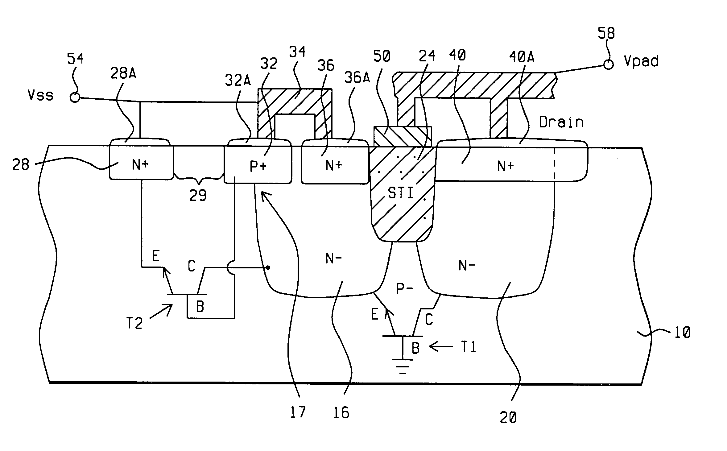
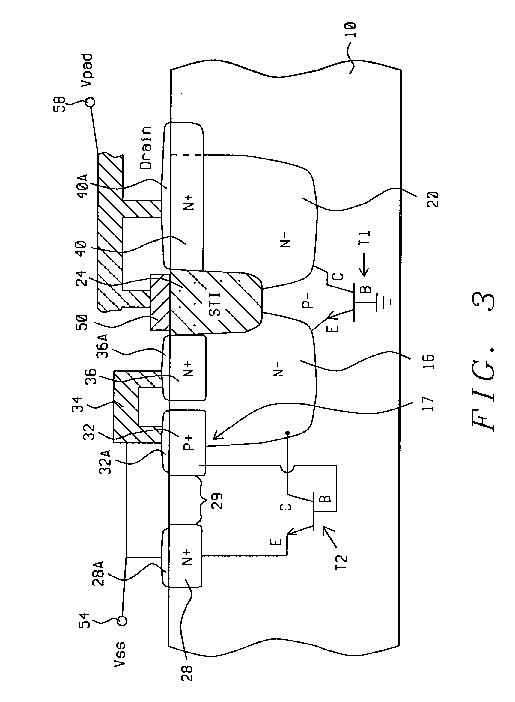
[0054] C. Third Embodiment
[0055] As shown in FIG. 3, the third embodiment contains the same elements as the second embodiment with the addition of a third n+ region 28. As shown in FIG. 3, a second NPN bipolar (T2) is formed: collector (e g., N+ 36, N- well 16), base (p+ 32 and P- substrate 10) and emitter (N+28).
[0056] The method of the third embodiment is similar to the second embodiment with the additional step(s) of forming the a third n+ region 28.
[0057] The third n+ region 28 is preferably shorted (or connected 34) to the first p+ region 32 and the second n+ region 36. Also, all the n+ and P+ regions have silicide regions overlying (e.g., 28A silicide).
[0058] Circuit Analysis for the 3.sup.rd Embodiment
[0059] The device can go into snap back mode because of the third n+ region 28.
[0060] The 3.sup.rd embodiment's ESD device forms two parasitic bipolar transistors. The first Tx (T1) is the same as in the first and second embodiment. The second parasitic bipolar Tx (T2) is made u...
PUM
 Abstract
Description
Claims
Application Information
 - R&D
- Intellectual Property
- Life Sciences
- Materials
- Tech Scout
- Unparalleled Data Quality
- Higher Quality Content
- 60% Fewer Hallucinations
Browse by: Latest US Patents, China's latest patents, Technical Efficacy Thesaurus, Application Domain, Technology Topic, Popular Technical Reports.
© 2025 PatSnap. All rights reserved.Legal|Privacy policy|Modern Slavery Act Transparency Statement|Sitemap|About US| Contact US: help@patsnap.com